CSCI 2150
Fall 2001 Test 2 -- Answers
The following is the answers to the Fall 2001 CSCI 2150
Test 2. In some cases, where the HTML does not prohibit it,
I've elaborated on the process to get to the answers.
- Fill out the truth table to the right for all possible
combinations of inputs for the circuit below. (Circuit not shown in answer sheet.)
Answer:
| Inputs | Outputs |
| ^S | ^R | Q | ^Q |
| 0 | 0 | illegal |
| 0 | 1 | 1 | 0 |
| 1 | 0 | 0 | 1 |
| 1 | 1 | Q0 | ^Q0 |
- Fill in the truth table for the XOR circuit
shown to the right. (Circuit not shown in answer sheet).
Answer:
- True or false: The D flip-flop with inputs CLK and D has no invalid states.
Answer: This question was probably not worded as well as it could've been.
It probably would've been better as "True or false: The D flip-flop with
only two inputs CLK and D has no invalid states." The answer is
true.
- How many D flip-flops are contained in an 8-bit RAM with 16
address lines?
Answer: If each memory location has 8-bits, then each memory location
has 8 flip-flops. With 16 address lines, then there are 216
possible locations. Therefore, the answer is 8 * 216 = 524,288.
Leaving the answer as an equation would've been fine.
- In a truth table, the symbol (arrow pointing upward) indicates that
the input is:
Answer: changing from a 0 to a 1 (rising edge).
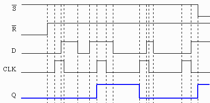
- Show the D flip-flop output waveform Q for the inputs ^S, ^R,
D and CLK indicated in the figure below. Assume the flip-flop captures
on the rising edge.
Answer: Note that the ^R = 0 at the first part of the graph eliminates
the unknown portion of Q before the first clock pulse and that the ^S = 0
at the end forces Q back to 1.

- Create the next state truth table for the state diagram below. (Diagram
not duplicated in answer key.) Use the variable names S1 and
S0 to represent the most significant and least significant bits
respectively of the binary number identifying the state..
Answer:
| Inputs | Outputs |
| S1 | S0 | A | S1' | S0' |
| 0 | 0 | 0 | 1 | 0 |
| 0 | 0 | 1 | 0 | 0 |
| 0 | 1 | 0 | 1 | 0 |
| 0 | 1 | 1 | 0 | 0 |
| 1 | 0 | 0 | 0 | 1 |
| 1 | 0 | 1 | 0 | 0 |
| 1 | 1 | 0 | X | X |
| 1 | 1 | 1 | X | X |
Questions 8 through 11 use this figure.

- If the current state is "run" and the input, K, equals 1, what
is the next state?
Answer: "wait"
- If the current state is "start" and the input, K, equals 0, what is the
system's current output?
Answer: "1" (Note that the input has no effect on the answer to this question.)
- Identify the error in this state diagram? Be as specific as you can.
Answer: The state "fault" has two transitions coming from it
with an input value of K=0 and no transition with a K=1 input. This is
an error.
- How many flip-flops would it take to realize this state machine?
Answer: To begin with, the diagram has 5 states, therefore, it will take
as many flip-flops as necessary to number 5 states with unique identifiers.
If you number the states, you should come up with a list
going from 0 to 4. And what is 4 in binary? 100. Since it
takes 3 bits to represent 4, then three flip-flops
are going to be required to remember 5 distinct states. Another
way of looking at it is that 1 flip-flop can remember 21=2 states,
2 flip-flops can remember 22=4 states, and
3 flip-flops can remember 23=8 states. 1 or 2 flip flops
is not enough. Three is the first value that has more than
5 possible states.
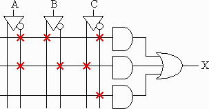
- Using the shorthand notation, set the PAL diagram to the right to
represent the boolean expression X = ^A B ^C + ^A ^B C + ^C.
Answer:

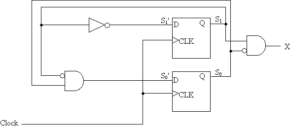
- The three Boolean expressions below represent the next
state bits (S0' and S1') and the output bit (X) based on the
current state (S0 and S1). Draw the logic circuit for the
state machine including the flip-flops and output circuitry. Be sure to label
flip-flop inputs and other signals.
S0' = S0 ^S1
S1' = ^S1
X = ^S0 S1
Answer:

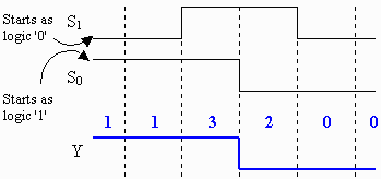
- For the multiplexer/selector shown to the right (Diagram not duplicated
in answer key), sketch the output waveform Y for the inputs S0 and S1 shown
in the graph below. Assume S1 is the most significant bit.
Answer: Note that the blue numbers indicate which of the D channels is being
selected.

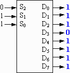
- For the active-low output decoder shown to the
right (Diagram not duplicated in answer key), fill in the values for all of
the outputs D0 through D7. Assume S2 is
most significant bit.
Answer:

- Circle all that apply. A storage cell in a SRAM:
Answer: a.) is volatile and d.) is a D flip-flop
- Circle all the memory types below can
only be written to with a programmer.
Answer:
c.) EPROM and e.) OTPROM
- Which of the following is best for very high volumes of
product to store code in?
Answer: c.) Custom-masked ROM
- Which of the following can be used like a miniature solid-state
hard drive?
Answer: b.) Flash RAM
- True or False: One memory block can have a low address of
AC0016 and a high address of AFFF16?
Answer: True. First, convert both the low and the high addresses to binary
to determine the pattern of 1's and 0's for the chip select.
AC0016 = 10101100000000002 and
AFFF16 = 10101111111111112. Since the first six
bits for both values are identical and the last 10 bits are all zeros for
the low address and all ones for the high address, then these two addresses
can most definitely be the high and low addresses for a single block of
memory.
- Using logic gates, design a chip select for a 128K RAM placed
in a 4 MEG memory space with a low address of 38000016. Label all
address lines used for chip select.
Answer: First, 4 Meg means that the total number of address lines coming
from the processor is 22 (A0 to A21). Second, since
the size of the RAM chip is 128K, the RAM chip will take 17 address lines
(A0 to A16). Therefore, the chip select will use
address lines A17 to A21. Converting 38000016
to binary gives us 11100000000000000000002. Using this binary
value, we can see that A21=1, A20=1, A19=1,
A18=0, and A17=0. (Note: since there are 22 lines from
the processor and 17 must go to the RAM, then 22-17 = 5 lines must be left
to go to the chip select. This checks out with our work.) The diagram
is shown below.

Created by David Tarnoff for use by his sections of CSCI 2150.
