Number of visits:
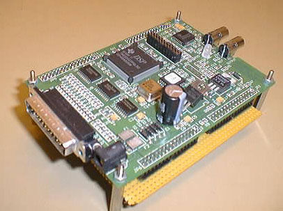
These are just some pictures and hints that might be of help to anyone who wants to add external fast memory to the C31 DSK. The design on this page adds 64 kwords of memory, that is, 256 kbyte, using four 15 ns SRAM chips borrowed out of a common 486 PC. I made the expansion while I did my thesis work, a DSP based MPEG-audio decompressor.
The DSK board has the entire DSP bus and control signals available at the edges. This make it trivial to add devices, provided that the address decoding can be made smoothly. Since I wanted a zero-waitstate design, and the 50 mhz DSP runs at 40-ns external cycles with a need for 9 ns H1 low to address valid, and 10 ns data setup before next H1 low (see table 13-13 on page 13-33 in the C31 manual), the memory needs to have an access time of 40-9-10=21 or less. Wire delay also plays a role so 15 ns memories should be used. Fortunately, fast SRAM's are readily available at speeds of 15 ns due to their popularity in older PC motherboards. The data bus width is 32 bits, so four 8-bit chips are needed. Common SRAM sizes are 32kbyte and 64kbyte, so four of those chips are needed. I used 64kbyte chips.
The databus and R/W signals can be wired naively directly to the DSP bus.
Now, the DSK is designed to allow for external memory at addresses 0x808000 and upwards. Fortunately, the DSP has a signal, /STRB, which is active only when the DSP knows that an address requires external access. This means that accesses to addresses 0x800000-0x807fff doesn't generate a /STRB. The result of this is that we can decode the external memory onto 0x800000 and upwards, if we use /STRB as a chip select. Decoding "0x800000 and upwards" is trivially done by using A23 as a chip-select. The 64kbyte SRAM chips happen to have two chip select inputs, one inverted (/CE1) and one non-inverted (CE2) so we can do this decoding without gluelogic at all! SRAMs like those use CS-controlled write cycles and thus we can tie /OE to ground permanently.
The result will be that the external memory is visible from 0x808000 and upwards. If you use 64kbyte chips, the memory repeats every 0x10000 so its easiest to use the memory as if it is between 0x900000 and 0x90FFFF. (0x808000 to 0x80FFFF will of course then be a mirror to 0x908000 to 0x90FFFF).
To sum it up:
| TMS320C31 | The four 64kbyte SRAM chips |
| D0-D31 | D0-D7/D8-D15/D16-D23/D24-D31 |
| A0-A15 | A0-A15 (A0-A14 for 32kbyte chips) |
| R/W | /WE |
| /STRB | /CS1 |
| A23 | CS2 |
| GND | /OE, GND |
| +5V | +5V |
If you only find 32 kbyte chips, it might be trickier since they might not have dual chip selects. You can't afford glue logic in a zero wait state design like this, so you need to figure out if it breaks something in the DSK if you map the memory without the A23 included. That would effectively put the memory at all external memory locations between 0 and 0xffffff, since it'd only decode /STRB. That might work, it definitely works on a non-DSK C31 board, but some I/O in the DSK might be upset.
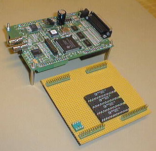
I made the expansion as a piggy-back wirewrapped board. This worked flawlessly, and the flanks look very well, despite the wire-wrapping of 25 mhz signals. Four box-headers need to be soldered to the sockets on the DSK, and four corresponding pin-headers need to be placed on the memory board. The following picture shows that design, before the two boards are connected together.
You need to figure out the actual pinout yourself, the DSK pinout is in the DSK schematics in the manual, and the SRAM pinouts are in the datasheets from the manufacturers. They are often standardized though, I used the pinout from a Motorola 64kbyte 15ns SRAM I found at Motorolas website, despite the fact that my chips weren't Motorola at all. If they have the same number of pins and same packaging, chances are good that it'll work :) Samsung have a 64 k * 8 chip as well that has the same pinout - you can download the PDF file for that at Samsungs site.
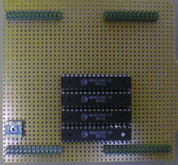
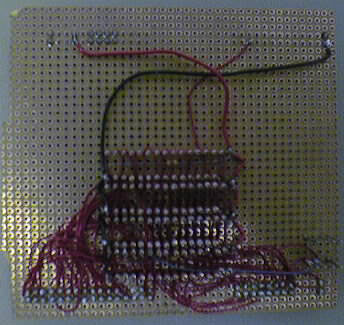
Below are two pictures of the top and bottom side of the memory expansion board. Sorry for the bad picture quality, I had to turn off the flashlight to prevent reflections.
Be sure to use thicker (non wire-wrap) cables for the GND and +5V connections. Use as short wirewrap cables as possible for the bus connections. Solder 100nF capacitors directly across the GND/+5V pins on each chip.
Apart from the physical design and connection, you also should configure the DSP for 0-waitstate operations. The DSK kernel defaults to using 2 waitstates, but the DSK works perfectly with 0 as well. This is set in a register in the C31 DSP that I can't remember right now, but it's easy to find in the manual. There are 3 bits that set the number of waitstates from 0 to 7, just set them to 0.
If you use the great C3x/C4x port of GCC and binutils made by Michael Hayes, a useful tip is to write an ld script which defines text and data segments in internal and external RAM. I have ".text", ".text2", ".data", ".data2" and with that it's easy to define in the assembler files which functions should go in which ram. If you use C, you can use the ld script to say where the text and data segments of every .o file should go.
Remember the segment register if you use data in both 0x80xxxx and 0x90xxxx areas.
See ya
Bjorn Wesen