Answers Database
FPGA Express: Instantiating an EDIF from a Foundation Schematic into a top-level FPGA Express Verilog or VHDL Design

Record #3010

Product Family:  Software

Product Line:  Synopsys

Problem Title:
FPGA Express: Instantiating an EDIF from a Foundation Schematic into a
top-level FPGA Express Verilog or VHDL Design


Problem Description:
Keywords: Foundation, FPGA Express, EDIF, module, modular, instantiate,
	  Verilog, VHDL

Urgency: Standard

General Description:

Using F1.3 or F1.4 and FPGA Express 1.2 or 2.0, it is possible to create an
EDIF file in Foundation, and instantaite this EDIF file in FPGA Express
Verilog or VHDL code.

This solution applies to both FGPA Express 1.2 and 2.0.  There are some
differences in these versions that are noted in the Solution below.
Steps 9, 10, and 14 can be skipped by Express 2.0 users.  Also, Steps 10 and 14
can be skipped by VHDL users, regardless of the version of Express used.


Solution 1:

(1) Create a project in Foundation.  Give the project the same name you want to
use for instantiating the schematic in the HDL code.  If the project name is
'big', then in Verilog the module name for the instantiated schematic is 'big'.


(2) Create a schematic in Foundation.  This schematic must have no I/O cells
like IBUF, OBUF, OBUFT, etc.

(3) In the schematic, use I/O terminals in place of I/O cells, as if were a
lower level of hierarchy.  The name of the I/O terminals will be the name of
the pins used for instantiation in the HDL code:


 Figure 1- 'test1' design with I/O Terminals

(4) After creating the schematics for the design, create an EDIF file by
selecting 'Options->Export Netlist'.  This will create an EDIF file in the
Foundation project.  The EDIF file will have the extension .edn and the
project name will be the name of the EDIF file.

(5) Place the EDIF file with the XNF files from FPGA Express in the same
directory in the project.

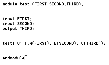
(6) For Verilog, instantiate the Foundation schematic, using the project
name as the instantiated module name, and the name of the I/O terminals as
the name of the pins.  In this example, the EDIF file was created in a project
called test1:


Figure 2-  Verilog Instantiation Example

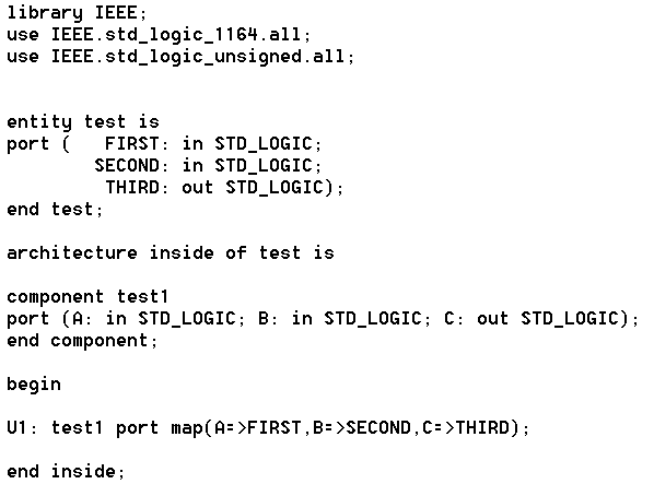
(7) For VHDL, instantiate the Foundation schematic, using the project name
as the instantiated module name, and the name fo the I/O terminals as the name
of the pin.  In this example, the EDIF file was created in a project called
test1:


Figure 3-  VHDL Instantiation Example

(8) Take all Verilog/VHDL design files, read, analyze, and implement the
design in FPGA Express.

(9) FPGA Express 1.2 ONLY: After implementing the design, select the
implementation window and select 'modules'.  The instantiated XNF module will
show up as 'UNLINKED'.	Preserve all instnatiated 'UNLINKED' modules.

(10) VERILOG ONLY, FPGA Express 1.2 ONLY: If one more the ports of the
instantiated EDIF are connected to a top-level port, the 'pad' direction must
be specified.  Select the 'Ports' tab in the Implementation window and define
the 'pad' direction (input, output, inout, or 3-state) for any EDIF
instantiated ports connected to top-level Verilog module ports.  Ports of the
EDIF not connected to a top-level port do not need to have a 'pad' direction
specified.

(11) Set all consraints for the rest of the design.

(12) Optimize the design.

(13) Write out the XNF file.

(14) VERILOG ONLY, FPGA Express 1.2 ONLY: Edit the pin directions of the
instantiated EDN file in the XNF file written by Express 1.2.  When Express 1.2
writes out an XNF file that contains instantiated black-boxes, Express 1.2
writes out the pin directions for the black-boxes as 'B'.  These pin directions
must be corrected to the proper direction for the given black-box.  PIN
directions can be I (input), O (output), or B (bidirectional).

(15) Take the XNF files from Express and the END file from Foundation and
process with M1.

Note, this procedure will work if a user wants to instantiate an entire
Foundation schematic based design with hierarchy.  The caveat the user must
follow is that the entire design must be a schematic, including all levels of
hierarchy.


Miscellaneous Tips

(1) If the EDN module to be instantiated in FPGA Express contains I/O elements
(IBUF, OBUF, OBUFT, IFD, etc.) care must be taken.  EDN modules with I/O for a
modular design will come in three types: modules with no I/O cells, modules
with I/O cells on all inputs and outputs, and modules with I/O cells on some
inputs and outputs.  FPGA Express v1.2 has the capability to isnert all the
I/O cells for a design, or none at all.  If the EDN has I/O cells in it, the
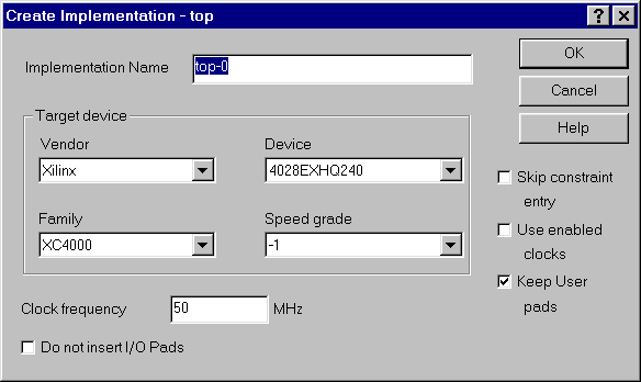
user must specify in FPGA Express not to insert I/O cells at all.  FPGA Express
can be prevented from inserting I/O cells by unselecting 'Do not insert I/O
Pads' box in the 'Create Implementation' Window in Express:


Figure 4-  I/O not inserted

(2) FPGA Express will be unable to apply logical and timing constraints for
logic contained within an instantiated EDN file.  The methodology for
instantiating an EDN file in FPGA Express places a hole in the HDL/netlist.
Since the contents of this 'hole' are not visible to FPGA Express, FPGA Express
will be unable to apply M1 constraints to this module.

(3) The M1.3 core technology software, like Verilog, is case-sensitive with
respect to names.  VHDL is not case-sensitive, but the XNF written out by FPGA
Express will follow the case-sensitivity used in the Verilog or VHDL code.
If case-sensitivity is not followed consitently when making constraints, the
M1.3 software may not be able to properly merge FPGA Express v1.2 XNF with
EDN files from Foundation 1.3.


End of Record #3010

| For the latest news, design tips, and patch information on the Xilinx design environment, check out the Xilinx Expert Journals! |


