Answers Database
FPGA Express v1.2/Foundation 1.3: Simulating with FPGA Express v1.2 HDL and F1.3 Logic Simulator

Record #3018
Product Family: Software
Product Line: Synopsys
Problem Title:
FPGA Express v1.2/Foundation 1.3: Simulating with FPGA Express v1.2 HDL
and F1.3 Logic Simulator
Problem Description:
Keywords: Foundation, FPGA Express, gate-level, simulator, Verilog, VHDL
Urgency: Standard
General Description:
FPGA Express is a synthesis only tool. It is possible to use the Foundation
gate-level simulator to perform functional and timing simulation on a design
synthesized with FPGA Express. There are 6 types of HDL designs that can be
simulated with the Foundation Simulator:
(a) pure HDL code
(b) HDL code with instantiated LogiBLOX
(c) HDL code with instantiated LogiCORE
(d) HDL code with instantiated XNF
(e) HDL code with instantiated EDF from F1.3
(f) HDL code which is a combination of one or more of b, c, d, and/or e.
Based on these design types, and based upon the Foundation-Express project
structure a user must follow, the Foundation gate-level simulator can
simulate an HDL based FPGA Express design.
Note: This solution is valid for FPGA Express 1.2 or 2.0.x with
Foundation F1.3 or F1.4.
Solution 1:
Overview of the Foundation-Express Project Structure
NOTE: In order to simulate an FPGA Express HDL design with Foundation, the
user must follow this project structure.
Overview of the F1.3/F1.4 Project Structure
In Foundation, when a project is defined, a user must specify the project name
and the location of the project directory. Within the selected project
location, a directory named after the project name will be created along with
a .pdf file (not an Adobe Acrobat file). The .pdf file contains project
information regarding the design files and libraries in the project.
After defining the project in Foundation, files can be added to the project by
selecting Document -> Add. Design files for a project can reside in any
location. In the interest of organization, the user's design files should
occupy the directory named after the project.
Overview of the FPGA Express Project Structure
Like the Foundation project manager, the user must specify the name and
location of a project in FPGA Express. The project name becomes a directory
inside the project location. Inside the directory named after the project,
FPGA Express creates two items: a 'Workspace' directory which is used by
FPGA Express during synthesis, and an .exp file, which contains project
information. Design files for a FPGA Express project can reside in any
location, but the user should place files in the project directory. Similarly,
after synthesizing a design, a user may place the resulting XNF file in any
location. The XNF file written by FPGA Express should be placed in the
Foundation project directory.
Foundation-Express Project Structure (Follow this setup for simulating a design
with Foundation)
(1) Start the Xilinx Foundation Project Manager
Figure 1- Foundation Project Manager Icon
(2) Select File->New Project to create a new project in the directory of choice.
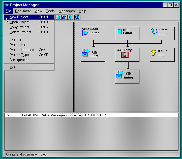
Figure 2- Defining a 'New Project' in the Foundation Project
Manager
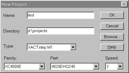
Figure 3- Specify Project Name
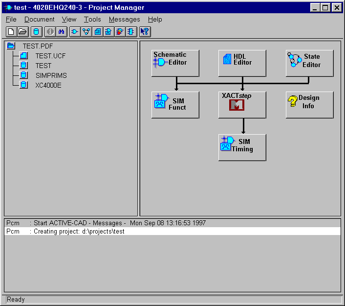
Figure 4- Foundation Project Manager Project Defined
(3) Using the Windows Explorer, create a subdirectory called 'express' inside
the directory where the Foundation project was created.
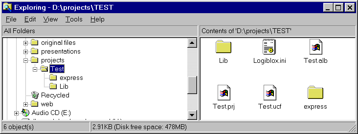
Figure 5- Creating the 'express' subdirectory
(4) Using the Explorer, copy all the HDL files inside the 'express'
subdirectory. Create any additional/new HDL files within this directory, too.
(5) Start FPGA Express and create an FPGA Express project inside the 'express'
subdirectory.
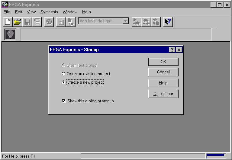
Figure 6- Making a new FPGA Express Project
(6) Add files to the FPGA Express project from the 'express' directory.
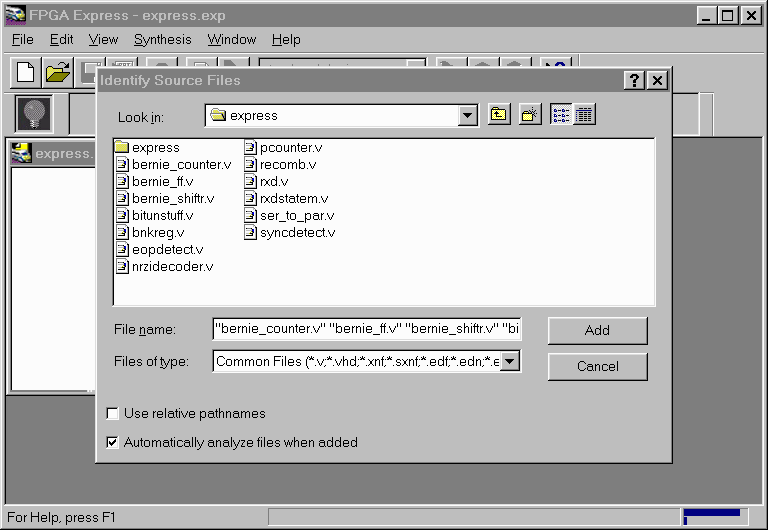
Figure 7- Adding HDL files to a FPGA Express Project
Solution 2:
Using the Foundation Logic Simulator to Functionally Simulate an FPGA
Express-based Design
(1) Create a Foundation-Express project structure. See Resultion 1.
(2) When generating the XNF file from FPGA Express, make sure that the XNF
file is saved into the Foundation-Express project directory. In this example,
this directory is d:\projects\test.
When using the Foundation Logic Simulator for functional simulation, there are
two possible flows to use, depending on whether the design's top-level is HDL,
or Foundation schematic.
Flow#1:
Simulate a Foundation Schematic with instantiated XNF modules from FPGA Express
(1) Create XNF files from Express for use in a Foundation schematic.
See (Xilinx Solution 3013).
(2) To functionally simulate the design, invoke the Foundation simulator by
clikcing the 'SIM Funct' button in the Foundation Project Manager, and simulate
as with any other Foundation design.
Flow#2
Simulate a Top-level HDL Express Design usin the Foundation Logic Simulator
(1) Invoke the Xilinx M1 Design Manager from the Xilinx Program Group.
(2) Create a new project, using the XNF file from Express as the input file.
(3) Create a new version and then a new revision, bu selecting
Design ->New Version, then Design->New Revision from the Design Manager.
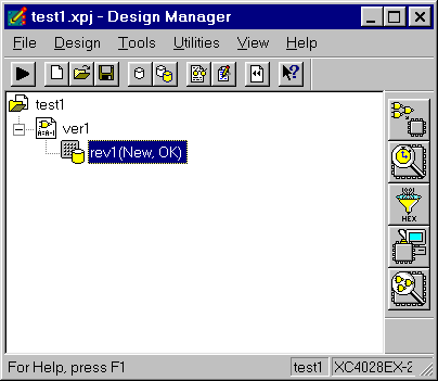
Figure 8- New Version and Revision created
(4) Run the Flow Engine and stop after 'Translate'.
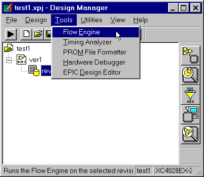
Figure 9- Run the Flow Engine
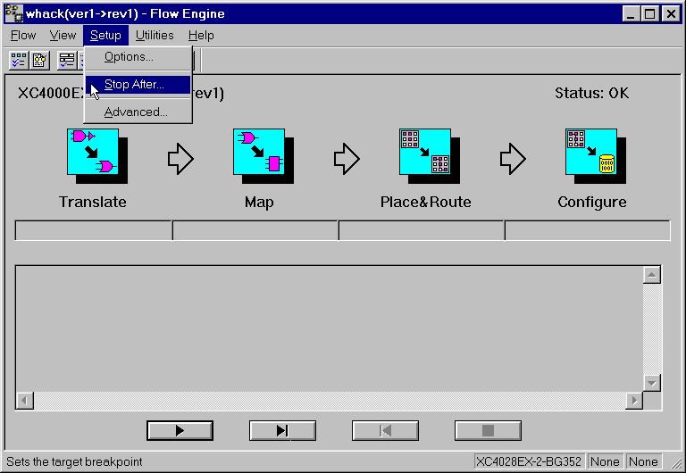
Figure 10- Set the Flow Engine to 'Stop After' Translate
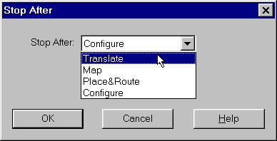
Figure 11- Setting the Flow Engine to 'Stop'
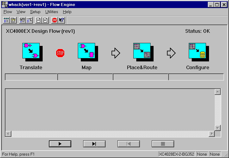
Figure 12- Flow Engine set to 'stop' after Translate
(5) Now, hit the 'play' button in the Flow Engine.
(6) When the Flow Engine is finished, go back to the Foundation Project Manager
and select Tools->Checkpoint Simulation.
An ngd file will appear in the Checkpoint Simulation Window. The file name
has the same nae as the device family of the project. The extension is .ngd.
In this example, since the project's device family is the 4000EX, the .ngd
file created was XC4000EX.ngd.
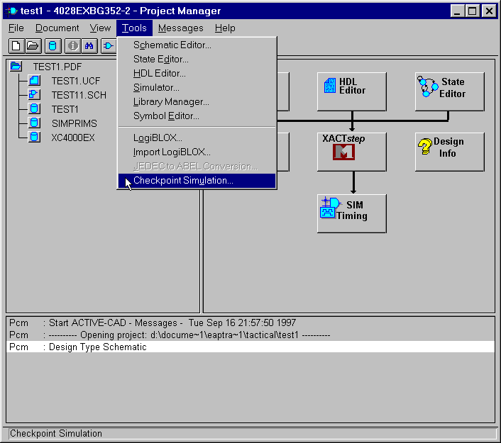
Figure 13- Checkpoint Simulation
(9) After selecting 'OK' in the Checkpoint Simulation Window, the Project
Manager will indicate that ngd2edif is running. When ngd2edif is finished,
the Foundation simulator will automatically start. Proceed with simulation
by selecting the signals to stimulate with Signals->Add Signals. The signals
listed will correspond to the top-level entity ports in VHDL, or top-level
module ports in Verilog. For more information on using the Foundation
Simulator, consult the Foundation Online Help.
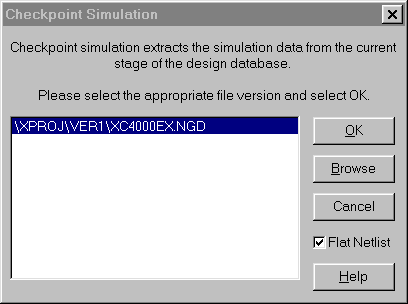
Figure 14- Select 'OK" to convert .ngd file to EDIF
Solution 3:
Timing Simulation using the Foundation Logic Simulator
(1) Create a Foundation-Express project. See Resolution 1.
(2) Place and route the design. In the Flow Engine, make sure that the
'Product Timing Simulation Data' is selected. If it is not, select
Setup->Options and check this option.
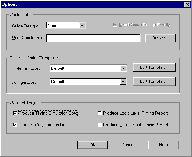
Figure 15- Creating Timing Simulation Data
(3) After placing and routin the design in the Design Manager, return to the
Foundation Project Manager and select Tools->Checkpoint Simulation.
(4) Select the appropriate <design>.nga file.
(5) Foundation will automatically translate this back-annotated timing
netlist to an EDIF File, and load the simulator.
End of Record #3018
| For the latest news, design tips, and patch information on the Xilinx design environment, check out the Xilinx Expert Journals! |