![]()
by Gregory R. Goslin
Corporate Applications Engineer
Xilinx, Inc.
Overview:
Traditionally, digital signal processing (DSP) algorithms are most commonly implemented using general-purpose (programmable) DSP chips for low rate applications, or special-purpose (fixed function) DSP chip-sets and application-specific integrated circuits (ASICs) for higher rates.
Technological advancements by Xilinx in Field Programmable Gate Arrays (FPGAs) in the past 10 years have opened new paths for DSP design engineers. The FPGA maintains the advantages of the high specificity of the ASIC while avoiding the high development costs and inability to make design modifications after production. The FPGA also adds design flexibility and adaptability with optimal device utilization conserving both board space and system power which is often not the case with DSP chips. When the design is demanding more than 100 MIPS, time-to-market critical or design adaptability is crucial the Xilinx FPGA is a great solution.
The SRAM based architecture of the Xilinx FPGA is well suited for Multiply & Accumulate (MAC) intensive DSP functions. A wide range of arithmetic functions for fast Fourier transforms (FFTs), convolution and filtering algorithms as well as the surrounding peripheral circuitry can be implemented into the Xilinx FPGA and reconfigured on-the-fly. When designing a DSP system in an FPGA the data can be processed taking advantage of single chip paralleled structures and arithmetic algorithms to exceed the performance of a single general-purpose DSP device.
Distributed Arithmetic[2] used for array multiplication is just one of the approaches used to increase data bandwidth and the throughput as much as several order of magnitudes greater in FPGAs than that possible in off-the-shelf DSP solutions. One example is a 16-Tap, 8-Bit Finite Impulse Response (FIR) filter[3]. It can support more than 780 MIPS at 5 million samples per second while occupying less than 2,100-gates or 70% of the 100 CLBs in an XC4003 device. Another example is a 64-Tap, 8-Bit FIR filter. It can support more than 3 GOPS at 5 million samples per second. Note that increasing the number of Taps has no significant impact on the sample rate when Distributed Arithmetic is used; see Figure 4-B. These two examples can also be implemented using a parallel Distributed Arithmetic algorithm to obtain sample rates of 50 million samples per second.
Now let's compare the 16-Tap FIR filter implemented in a state-of-the-art fixed-point DSP with that of the Xilinx FPGA. As published by Forward Concept, "For 1995, the state-of-the-art fixed-point DSP is rated at 50 MIPS." Consider the same device which requires 20 nsec per Tap to implement a 16-Tap FIR filter, which translates to a maximum sample rate of 3.125 million samples per second. General-purpose DSP devices have a significant decrease in performance measured by the device's MAC cycle time per Tap, as shown in Figure 4-A. If you are designing a system which requires one or more traditional DSP devices, consider performance advantages available with Xilinx FPGAs.
Xilinx In-System Programmable (ISP) FPGAs can be reconfigured while on the board. Taking advantage of the reconfigurability feature means a minimal chip solution can be transformed to perform two or more functions. Take for an example a system that performs one of several DSP functions. Suppose for instance one function is to compress a data stream when in transmit mode and another function is to decompress the data when in receive mode. The FPGA can be reconfigured on-the-fly to switch from one function to another. This capability of the FPGA adds a lot of functionality to a down-sized DSP system controlled by a small logic translation circuit. The reconfiguration of the FPGA can also be taken advantage of in board level products that use only one or a subset of the many standardized bus interfaces. If an FPGA houses the interface circuitry, than the FPGA configuration PROM can be changed to support the configuration specified by the bus standard without making printed circuit board or design changes. This approach brings production level up and cost down for a given production run.
The FPGA design cycle requires less hardware specific knowledge than that required by most DSP chips or ASIC design solutions. Smaller design groups with less experienced engineers can be given the opportunity and trusted to design larger, more complex DSP systems in a shorter amount of time than that of larger design groups with more experienced engineers which are required to have knowledge of device specific programming languages. The FPGA design team can have a complex DSP system designed, tested, verified, and ready for production in weeks while the DSP chip and/or ASIC design teams could still be waiting for product design test results.
Multiply & Accumulate:
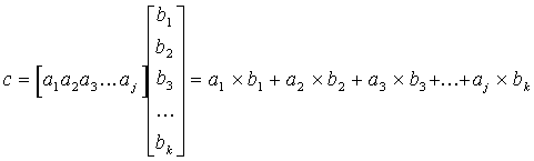
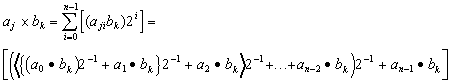
In many DSP functions, Multiply and Accumulate (MAC) is used to define the function. Mathematically the MAC is represented by the multiplication of two matrices, a matrix or vector by a scalar which implies each element of the vector is multiplied by the scalar. Two matrices, A and B, can be multiplied if the number of columns in A equals the number of rows in B. Let A be of order (m x n) (m-rows x n-columns) and B of order (n x p). The product of the two matrices C = AB, is the matrix of order (m x p) with elements
Equation 1:
![]()
This states that ![]() is a scalar product of the i'th row vector of A and the j'th column
vector of B.
is a scalar product of the i'th row vector of A and the j'th column
vector of B.
An example is a filtering function with Tap Coefficients A and Data samples B:
e.g.,
Since there is no dedicated multiplier in the FPGA architecture,
the ![]() terms must be subdivided
into more elementary terms. This is done in a fashion similar to that of
Equation 1. The process is a summation of partial products, as follows
terms must be subdivided
into more elementary terms. This is done in a fashion similar to that of
Equation 1. The process is a summation of partial products, as follows
Equation 2:
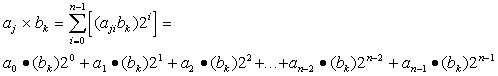
Where the multiplier (the number that multiplies), ![]() is a binary number n-bits wide and the multiplicand (the number to be multiplied),
is a binary number n-bits wide and the multiplicand (the number to be multiplied),![]() is a binary number m-bits wide, and i represents the bit placement.
is a binary number m-bits wide, and i represents the bit placement.
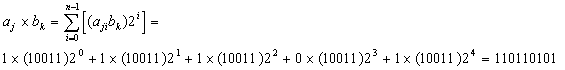
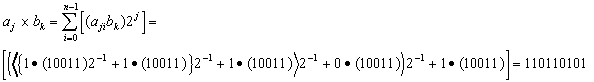
Example of two 5-bit unsigned binary numbers, ![]() =
= ![]() and
and ![]() =
= ![]() , such that,
, such that, ![]() x
x ![]() = c =
= c = ![]() :
:
It can be seen that Equation 2 is nothing more than a series of binary AND operations (multiplication) to determine an add or no-add decision followed by a shift and ADD function (accumulation). Equation 2 is a mathematical representation of a fundamental MAC. MACs can be implemented several ways in the FPGA. Checking the bits of the multiplier one at a time and summing partial products is a sequential operation that requires a sequence of add and shift sub-operations.
Array Multipliers are probably the most common. The multiplication of two binary numbers can be done with one sub-operation by means of a combinatorial circuit that forms the product bits all at once. This is a fast way of multiplying two numbers since all it takes is the time for the signals to propagate through the gates that construct the multiplication array. However, the array multiplier requires a large number of gates and for this reason it is not economical for MAC intensive applications. To see how the array multiplier can be implemented, consider the multiplication of two 2-bit numbers as shown in Figure 1. The Multiplicand bits are b1 and b0, the multiplier bits are a1 and a0, and the product is c3, c2, c1 and c0. The first partial product is formed by multiplying a0 by b1b0 . The multiplication of two bits produces a 1 if both bits are 1, else it produces a 0. This is identical to an AND operation and can be implemented with an AND gate. As shown in Figure 1, the first partial product is formed by means of two AND gates. The second partial product is formed by multiplying a1 by b1b0 and is binary-shifted, one bit to the left. The two partial products are added with two half-adders. When there are more bits in the partial product terms, full-adders will be necessary to produce the sum. Note that the least significant bit does not need to go through an adder stage since it is formed by the output of the first AND gate.
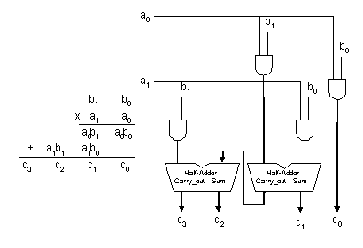
Figure 1 Array Multiplier for Two 2-Bit Numbers
An array multiplier with more bits can be constructed in a similar fashion. Each bit of the multiplier is ANDed with each word of the multiplicand in as many levels as there are bits in the multiplier. The output in each level of AND gates is added in parallel with the partial product of the previous level to form a new partial product. The last level introduces the product. For j multiplier bits and k multiplicand bits, j x k AND gates and (j - 1) k-bit full-adders are required to produce a product of j + k bits.
Equation 2 can be redistributed to be performed as a serial sequential summation of partial product terms, least-significant-bit (LSB) first, as follows
Equation 3:
The example of two 5-bit unsigned binary numbers, ![]() =
= ![]() and
and ![]() =
= ![]() , such that,
, such that, ![]() x
x ![]() = c =
= c = ![]() is processed as follows:
is processed as follows:
The implementation of Equation 3 has been canned as Distributed Arithmetic [2] and maps efficiently in the Xilinx FPGA architecture. Equation 3 can be implemented in several variations. It can be implemented as a serial sequential operation, in which each multiplicand is operated on independently, much like that of an array multiplier. This technique is best used when only one data value is being multiplied or the sample rate is very low, refer to Figure 2. Note that if the Multiplicand values are a predetermined set of constants. The Multiplicand value can be stored in a (2 x m-bit) RAM and use the RAMs one bit address to access the Multiplicand as needed with the serial output datum from the parallel to serial converter. In the RAM implementation, Address 0 would have a value of 0 and Address 1 would hold the value of the constant multiplicand.
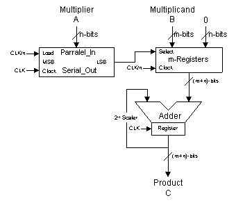
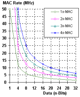
Figure 2 Serial Sequential Multiplier
Equation 3 can be implemented in various levels of parallel structures, in which an array of multiplicands are operated on in parallel by common or unique multipliers. It is the parallel structures that are most interesting. If the circuit illustrated in Figure 2 was repeated for n-bits then the multiplication would be performed at the clock rate. Example: If n-bit data is bit-serial sequentially processed at 50MHz the multiplication rate would be 50MHz divided by n-bits. For 16-bit data this would be 3.125MHz. If the process was performed 2-bits per clock cycle, then the multiplication rate would double. For 16-bit data this would be 6.25MHz. This process can be repeated up to n-times to perform the multiplication at the clock rate. The 16-bit data can be processed at 50MHz.
The process of multiplying an array of multiplicands by an array of multipliers is referred to as Serial Distributed Arithmetic when the array of multiplicands is operated on serial sequentially, LSB to MSB, by each bit of the multipliers, as shown in Figure 3. With this process, all possible combinations of multiplicand sums are precomputed and stored in a look up table. Each multiplier value operates on its associated multiplicand as follows:
The n-bit multiplier data A0 is loaded in parallel at the data rate of CLK/n. At this time, each serial shift register holds a unique multiplier value. The LSB from each serial shift register is used to address the look up table data. The data stored in the look up table represents all possible sums of the partial products of the multiplicands.
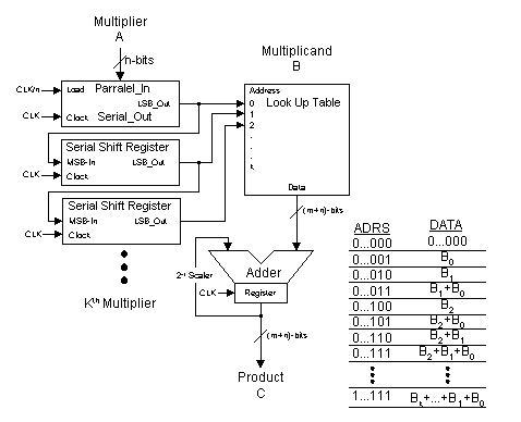
Figure 3. Serial Distributed Arithmetic
The Address of the look up table Data can be viewed as a binary mask. That is, each Address bit represents a unique multiplicand word B, such that, Address bit-0 corresponds to B0, Address bit-1 corresponds to B1, Address bit-2 corresponds to B2, until Address bit-k corresponds to Bk. If the Address bit-n is a 1, then the corresponding multiplicand Bn is included in the summation of product terms which is represented by the look up table Data output. If the Address bit-n is a 0, then the corresponding multiplicand Bn is not included in the total summation.
The Address ...000, holds a value of ...000, as it represents
the summation of zero product terms.
The Address ...001, holds the value of B0,
as it is the only product term in the summation.
The Address ...010, holds the value of B1,
as it is the only product term in the summation.
The Address ...011, holds the value of (B1
+ B0), as both B1 and B0
are product terms in the summation.
The Address ...100, holds the value of B2,
as it is the only product term in the summation.
The Address ...101, holds the value of (B2
+ B0), as both B2 and B0
are product terms in the summation.
The Address ...110, holds the value of (B2
+ B1), as both B2 and B1
are product terms in the summation.
The Address ...111, holds the value of (B2
+ B1 + B0), as B2,
B1 and B0, are product terms in the summation.
This pattern is continued until all Address bits are 1, in
which case the value of (Bk +...+ B2
+ B1 + B0) would be represented.
The advantages of Serial Distributed Arithmetic is in its ability to multiply arrays in a constant amount of time. The time, for such a process, can be magnitudes less than that required by traditional general-purpose DSP processors. Processor based multiplication requires a fetch, multiply and accumulate operation for each array element. Each processor instruction must be time multiplexed as a single processor can only do one operation at a time. This serial sequence of operations generally requires multiple clock cycles to perform just one multiply and accumulate.
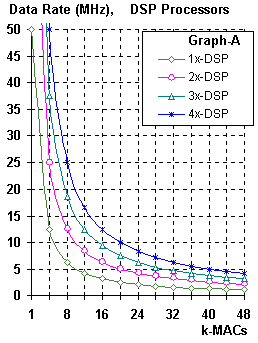
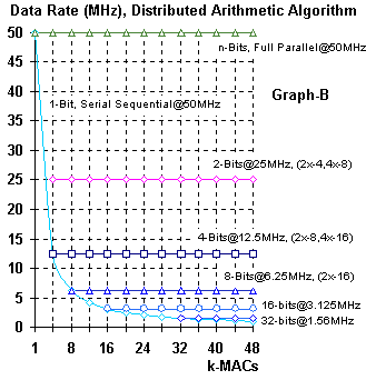
Figure 4. Data Rate Verses MACs @50MHz
The performance, of a processor based device, can be characterized by the maximum MAC frequency divided by the number of MACs required at the Data sample rate, as shown in Figure 4-A. It can be seen that a function requiring, for example, 20-MACs per Data sample that a single processor with a 50MHz MAC frequency could support a maximum Data rate up to 2.5MHz. Two 50MHz processors are required to support a 5MHz Data rate and perform 20-MACs per sample. Four 50MHz processors are required to support a 10MHz Data rate and perform 20-MACs per sample, etc.
Now Distributed Arithmetic starts looking really interesting. Evaluating the process used for Serial Distributed Arithmetic. It can be seen from Figure 2 and Figure 4-B, that the determining factor in the performance of Serial Distributed Arithmetic is the number of bits representing the multiplier or Sample Data. Once the sample rate is calculated, (maximum clock rate divided by number of multiplier bits) the MAC rate is constant, as shown in Figure 4-B.
The MAC frequency can be increased by processing multiple bits in parallel. This process is referred to as Parallel Distributed Arithmetic. First, processing two-bits per clock cycle, the Serial Distributed Arithmetic Data rate is doubled. An example is 16-bit Data can be multiplied, two-bits per clock cycle (2x-16), at a sample rate of 6.25MHz for any number of MACs per Data sample. This example is identical, in characteristics, to that of the 8-bit Data using single-bit Serial Distributed Arithmetic as shown in Figure 4-A. Secondly, processing four-bits per clock cycle, the Serial Distributed Arithmetic Data rate is quadrupled. This process can be continued until all of the multiplier bits are processed in parallel. This results in a full Parallel Distributed Arithmetic process. The full Parallel Distributed Arithmetic algorithm can process Data at the clock rate, or 50MHz for the examples given.
Implementing Distributed Arithmetic techniques in the Xilinx FPGAs can produce single chip solutions for complex, MAC intensive applications. These FPGA implementations can result in magnitudes of performance gain over multiple DSP device solutions. Filtering algorithms are ideally suited for Distributed Arithmetic. From the basic Finite Impulse Response (FIR) filter to complex image compression, with such techniques as Fast Wavelet Transforms (FWT). The FPGA is a DSP work shop where hardware solutions are within reach.
Custom Design Example, Digital Filtering:
A 16-Tap, 8-Bit Finite Impulse Response (FIR) filter, will be used as an example [3]. This example will be defined to be symmetric with constant coefficients, as shown in Figure 5. The FIR filter function will be implemented in a Xilinx XC4000 FPGA, as shown in Figure 6. The construction will be based on 8-Tap FIR filter building blocks to permit easy design reuse and expansion. The building blocks allow any multiple of 8-Tap FIR filters to be constructed with only minor changes to the control logic to support additional stages.
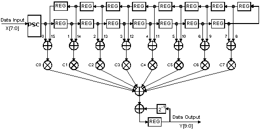
Figure 5 Data Flow Diagram for 16-Tap FIR Filter
The 16-Tap FIR filter has the data flow processing as follows. The Sampled Data is Registered in Parallel and then serially shifted LSB first at the clock rate. RAM Based Shift Registers are used to store all preceding Data bits. The use of RAM Based Shift Registers significantly reduces the overall size of the design compared to a cascade of serial registers.
The 16-Tap FIR filter design uses serial adders to sum the two taps with equal coefficients. This serial summation reduces the amount of logic used at the expense of one additional clock cycle, in reference to the implementation in Figure 3, to allow for serial summation over-flow. The total processing time is calculated as 20nsec x 9-bits = 180nsec = 5.55MHz (20nsec x (n+1)-bits). Once again, note the filter design is independent of the number of taps.
The eight output bits from the serial adders are used to address the ROM Based Look Up Table Data which represents the summation of all partial product terms. This is the same process as described for the Serial Distributed Arithmetic in Figure 3.
The Complementing stage is used for only signed data. When signed data is processed the most significant bit (MSB) is used to perform a 2's complement on the data. This is done by inverting the registered data and adding 1. Note that there are actually two numbers being complemented, one for each 8-Tap block. Hence, a 2 is added by adding a 1 at each of the two Full Adders.
The first Full Adder is used to add the two 8-Tap partial product summations. This registered data is the 16-Tap partial product summation.
The second Full Adder and associated circuitry builds a Scaling Accumulator. It is with in this block that the combined 16-Tap partial product terms are summed and appropriately weighted. This is done in the same manner as described for Figure 3. The output of the Scaling Accumulator is the Filtered Data.
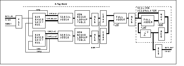
Figure 6 Block Diagram for Xilinx FPGA Implemented 16-Tap FIR Filter Function
To show the adaptability of the FPGA architecture the circuit in Figure 6 can be duplicated to process two 8-bit words in parallel and summed, observing the bit orientation of the high-word with respect to the low-word, to sample 16-bit data at the same frequency of 5.55MHz. This design can also be extended to a higher order of taps without a decrease in sample rate.
Another example would be the creation of a 32-Tap, 8-Bit FIR filter. The 16-Tap FIR filter in Figure 6, could be replicated and placed along side the original circuitry. Another Full-Adder and Register block would be added to sum and register the outputs from each 16-Tap block. Note that this added circuitry would also add one clock cycle of latency to the overall function and the control logic would need to be adjusted accordingly.
In summary, Table 1, is a list of the number of CLBs used to implement the 8-Tap, 8-Bit building block for various orders of FIR filters.
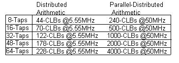
Table 1 8-Bit FIR Filter Order Versus Size
[1] Pratt, W. K. "Digital Signal Processing, Second Edition," Wiley-Interscience Publication, 1991.
[2] Mintzer, L. "Mechanization of Digital Signal Processors," Handbook of Digital Signal Processing, pp. 941-973, 1987.
[3] Goslin, G. R. & Newgard, B. "16-Tap, 8-Bit FIR Filter Application Guide," Xilinx Publications, 21NOV94.