Introduction
This application note illustrates the use of Spartan devices in an Asymmetric
Digital Subscriber Line (ADSL) modem. In this application the Spartan device
is used to implement the complex system level glue logic required for the
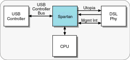
modems Universal Serial Bus (USB) interface. The Spartan device sits between
the CPU, USB interface controller, and the ADSL modem, and manages DMA transfers
of ATM cells. The design example shows how cost effective a Spartan device
can be in these applications.
ADSL technology can expand the useable bandwidth of existing copper telephone
lines, delivering high speed data communications at rates of up to 8 Mbps.
The recent G.Lite standard allows for a lower-speed, lower-cost implementation.
The USB interface is becoming the standard on both PC and Macintosh-based
platforms. This document assumes that the reader is familiar with ADSL,
USB and ATM
technologies.
While the design is targeted at solving a specific problem, interfacing
an ADSL chipset to USB, it illustrates solutions to a number of general
technical issues. These include implementing Utopia interfaces for ATM
devices and remote configuration of Spartan devices.
Overview
The design objectives for this application were threefold. First was the creation
of a solution with the lowest possible cost. In this case the target was
a semiconductor bill of materials for the USB interface that is significantly
less than $10 in volume.
The second objective was to deliver a solution that would deliver the
best possible performance. Current solutions are able to deliver 2 to
3 Mbps of bandwidth across USB at a much higher price point. The minimum
target for this design was to be able to support the full 1.5 Mbps data
rate of G.Lite and at the same time get as close to the full G.992.2,
6.1 Mbps data rate.
The third objective was to configure the Spartan device from the host
via the USB interface. This has the dual benefit of eliminating the requirement
for FPGA configuration memory in the modem and the ability to update the
configuration in the field.
Figure 1 ADSL Modem System Block Diagram
Before we examine the functions implemented in the Spartan device, lets
get a overview of the devices that were chosen for the ADSL PHY, USB controller,
and CPU blocks.
Alcatel Dynamite Chipset
The ADSL chipset chosen for this design is the Alcatel Dynamite chipset. This
three chip set consists of the MT-20134 Analog Front End, the MT-20135 ADSL
Modem and ATM Framer, and the MT-20136 ADSL Transceiver Controller. Of these
devices the Spartan device interfaces to the MT-20135, and MT-20136.
Figure 2 Alcatel Dynamite Chipset Block Diagram
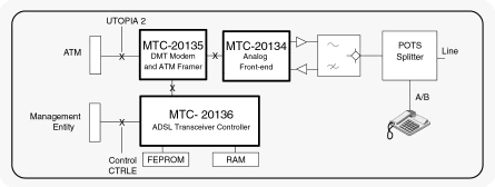
Figure Courtesy Alcatel Microelectronics
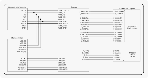
The MT-20135 sends and receives data in the form of ATM over a standard
Utopia level 2 interface. This interface was defined to transfer ATM cells
between physical layer devices like the MT-20135 and segmentation and
re-assembly (SAR) controllers or ATM switching fabrics. The function of
the Spartan device in this design is to handle the handshaking required
to convert the full duplex ATM cell stream from the Utopia interface into
half-duplex transfers to and from the USB controller. Since both the MT-20135
and the USB controller have internal FIFOs capable of storing a complete
ATM cell, the transfers consist of moving data one cell at a time between
these FIFOs.
The MT-20135 supports non-ATM transport schemes by way of another interface
referred to as the Synchronous Link Access Protocol (SLAP) interface.
The SLAP interface is not used in this application.
The MT-20136 contains an ARM processor, a memory controller, and an interface
bus that is connected directly to the MT-20135. The MT-20136 is essentially
a single chip processor dedicated to managing the ADSL modem. The Spartan
device interfaces to this device via a specialized management interface
that Alcatel refers to as CTRLE. This interface is used to control the
modem and to query status.
National Semiconductor USBN9602
The USB interface in the design is based on a National Semiconductor USBN9602
controller. This device, packaged in a 28 pin SOIC package, contains all
of the logic necessary to transfer data frames to and from the host with
minimal processor intervention. It contains several endpoint FIFOs, two
of which are 64 bytes deep. These FIFOs are large enough to contain a complete
53-byte ATM cell plus a control header if required.
Figure 3 National USBN9602 Block Diagram
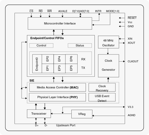
Figure Courtesy National Semiconductor The USB interface could be implemented in a Xilinx FPGA, but for this
application the dedicated USB chip provides the most cost-effective solution.
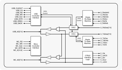
In this design the Spartan device contains logic to support two primary
functions. The first of these is DMA logic that manages the transfer of
ATM cells between the USBN9602 and the Utopia interface.
The second function is arbitrating access to the USBN9602 by an 8051
microcontroller. Although the bus on the USBN9602 is designed for direct
attachment to the 8051, doing so would eliminate the ability of the Spartan
device to directly transfer cells to and from the USBN9602. This is because
there is no mechanism available to force the 8051 to relinquish control
of the bus when the DMA logic in the Spartan device needs to perform a
transfer. Microcontrollers with this feature are significantly more expensive
than the 8051.
Microcontroller Selection
The microcontroller chosen for this design was an 80C51. This device is available
from multiple vendors and is very inexpensive. Aside from low cost, the
features that were required for this application were as follows:
- On chip ROM and RAM: to reduce parts count.
- External memory bus: to facilitate reading and writing registers in the USBN9602
and MT-20135
-
13 general-purpose I/O pins: used for accessing the USBN9602 before the
Spartan device is configured, more on this in the following section
Although the 8051 microcontroller meets these requirements, a variety of other
devices such as the Motorola 68HC11 could have been used.
The performance that is required of the microcontroller is minimal. This
is due to the fact that the Spartan device handles the real-time transfer
of ATM cells between the ADSL chipset and the USB interface. The functions
handled by the microcontroller include initializing the Spartan device
at startup and responding to status queries from the host received via
USB messages.
Spartan Device Selection
Spartan devices are available in a range of densities and packages. The following
criteria were used to select the device used in this application: |