Introduction
The underlying goal of this document is to introduce designers to the value
that Xilinx Programmable Logic can provide to the world of printers.
The approach we will take here is to basically build up the functionality
needed to make a mainstream ink jet printer, so the required functionality
is identified, and the performance improvement is understood for each refinement.
At the end of the process, we will outline a more ambitious solution by
embedding our work into the framework of MultiFunction Peripherals, a rapidly
emerging market frontier.
Overview
Most of today's printers have substantial onboard intelligence, to perform
various data decompression and refinement operations and off-load the host
processor. However, extremely low cost models still rely on the host
processor doing the compute intensive operations, hence, they slow down
substantially for elaborate text fonts or dramatic graphic images. We begin
the design overview by outlining the tasks to be performed and show several
design tradeoffs that move the intelligence from the host into the printer
controller. We will also discuss the nature of the added refinements,
so hardware and software requirements are appreciated by the reader.
Today's printer manufacturers cover a large number of companies.
Apple, Brother, Canon, Epson, Hewlett-Packard, Lexmark and Okidata are
large ones, but just a few of them. Many of them supply ASICs, print
engines and toners to the others. Today, most of them have embraced
microprocessors/controllers in the heart of their systems. In the
past, the Intel i960 was a strong embedded controller in printers.
After that, the Motorola 68000 family was prevalent. Lately, the
Motorola ColdFire family of RISC machines and the Advanced RISC Machine
(ARM) processors have become very popular.
One reason both ColdFire and ARM architectures have been popular is
that both fit the System On a Chip (SOC) processing model. In this
situation, a single chip performs computation and storage, with negligible
external support. Both architectures include a processor core surrounded
with substantial peripheral control circuitry to greatly reduce, but not
entirely eliminate, the need for additional "glue" logic to attach memory
modules or bus interface circuitry. Both processors operate at reasonable
speeds and have substantial power control circuitry to also fit the Energy
Star model of good power management. The ARM architecture also has
the added feature of being a well supported hard "core" that is included
in a large number of compute intensive ASSP solutions, some of which will
be mentioned later.
Before describing the solutions in more detail, let's examine the basic
tasks that will be needed for all the solutions. Then, we can best
see exactly how placing the intelligence in the printer offloads the host.
To begin, assume a file exists on the host and needs to be printed.
The host must drive the data out the I/O port (typically the parallel port)
and into the printer (via a Centronics or Bitronics IEEE 1284 connector/protocol).
If the design is simple, the data must arrive in pre-formatted condition
to be forwarded directly to the print engine controller. Specifically,
it needs to already resemble video data with explicit carriage returns,
nozzle identification, dithering, edge enhancement, high level motor controls,
etc. The printer controller chip we will use here is the Conexant
PIF-LM1. The PIF-LM1 is designed to attach directly to the
print engine and supply signals to stepper and DC motor drivers, the print
head drivers, the host system, print head position optical encoder and
General Purpose I/O (GPIO) ports for paper sensing, print head power management,
etc. Figure 1 shows the block diagram level of interface for the
PIF-LM1. It will be used for subsequent examples, so let's examine
it now.
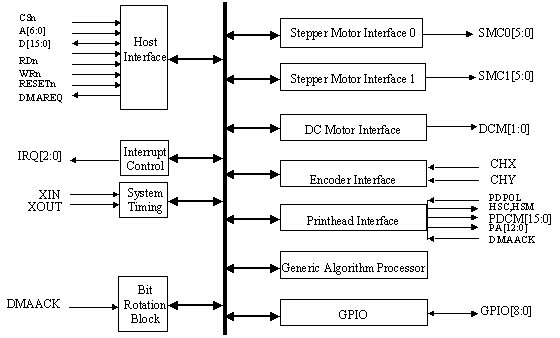
Figure 1: Architectural View of the Conexant PIF-LM1 ink jet
ASSP chip
Basic features for the PIF-LM1 include the following:
-
Resolution selection: single head 300, 600 dpi; dual head 600 X 600, 1200
X 600, 1200 X 1200 dpi
-
8/16 bit processor interface
-
Programmable interrupt control
-
DC Motor control with pulse width modulated speed control
-
Dual stepper motor control
-
Optical print head encoder control
-
Consecutive Dot Elimination (CDE) for draft printing
-
Programmable print dithering function (mono or color)
-
Programmable fire delay
-
Programmable nozzle fire
-
The generic algorithm processor handles tasks like PID control, programmable
interrupt and arithmetic calculations
-
Bit rotation block permits bidirectional printing, nozzle pitch and number
configuration.
Basically, the ordinary housekeeping tasks needed for ink jet management
are handled with the PIF-LM1. For brevity, we will refer to the PIF-LM1
as the "PIF". Figure 2 shows how the PIF interacts in a simple system.
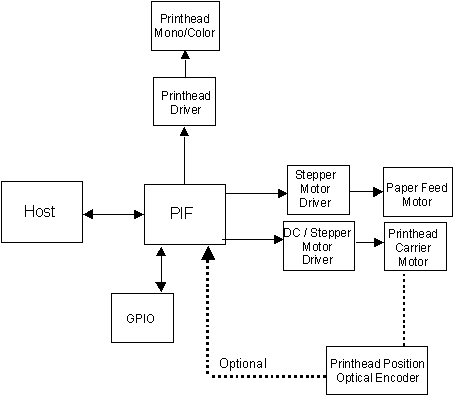
Figure 2: PIF-LM1 Embedded in an Ink Jet Printer
From Figure 2, the Host (PC) delivers the bitstream to be printed, with
embedded information like end of line, end of page, etc. The PIF
extracts the bitstream and delivers it directly to the print head drivers.
It also identifies the page feed and line feed info and delivers the commands
to the corresponding stepper motors. The PIF handles the direct attachment
to the functionality of the printer. Interfacing the PIF to the host
will be the first issue to be addressed.
A Basic Printer Interface
In this version, the host does most of the data management tasks.
Programmable logic is chosen as the interface between the host parallel
port and the PIF. In that sense, it is important that the data be
managed so that the PIF "sees" a host instead of just the parallel data
port. The basic task of the PLD is to collect bytes of data, form
command and data words for the PIF and create control strobes that drive
the information into the printer interface.
Eliminating the additional chips shown in Figure 2 and focusing on the
Host interface, we arrive at Figure 3, which shows an XC95144XL assuming
the tasks of the "host".
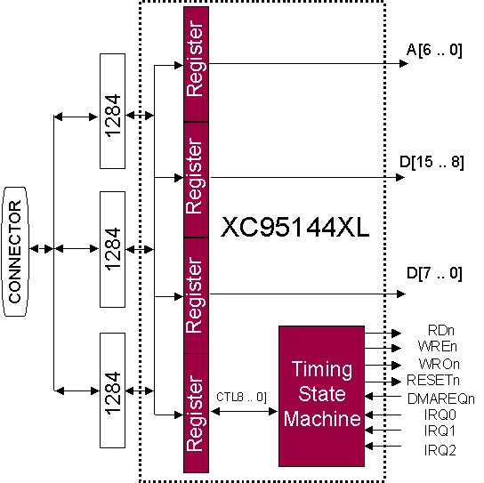
Figure 3: Basic CPLD Interface Solution
The direct electrical interface is done with the TI ACT1284 bus interface
chips, which meet the exact electrical requirements and provide a high
drive buffering capability as well as internal pull-up resistors.
The functionality for the CPLD is basically registering the data taken
off the parallel port connector (after buffering) and splitting out address,
data and control chunks. Then, the resulting address / data sets
need to be delivered to the PIF chip. A state machine is inserted
to resolve the interface timing differences between the IEEE 1284 timing
and the PIF. Typically, the functionality shown in Figure 3 might
occupy a smaller PLD ö say an XC9572XL, but remaining logic can be
used to drive LEDs and debounce switches that might be useful for manual
intervention. Figures 4 and 5 show basic data and address protocols
for the Enhanced Parallel Port version of the IEEE 1284 specification.
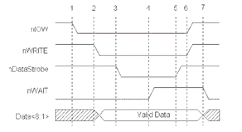
Figure 4: EPP Data Write Cycle (courtesy Warp Nine Engineering)
The Data Write handshake is very simple. The nIOW signal, nWrite
,nDataStrobe and nWAIT are all active low. As nWait rises, the Valid
Data transfers.
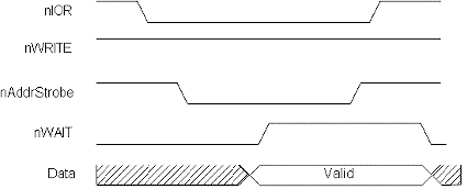
Figure 5: EPP Address Read Cycle (courtesy Warp Nine Engineering)
In Figure 5, nIOR, nWRITE, nWAIT and nAddrStrobe are all active low.
As shown, the valid data transfer occurs as nWAIT transitions high.
Signal speeds are well within the capabilities of the slowest programmable
logic, so timing is not an issue.
Adding Printer Description Language
Moving intelligence into the printer, dramatically offloads the host PC.
Typically, a PDL is used and either PostScript or PCL is the most natural
choice. Either way, we will insert a ColdFire microprocessor and
the current favorite is the MCF5307. Figure 6 shows
how addition of the processor with supporting DRAM and EPROM take local
intelligence right into the printer.
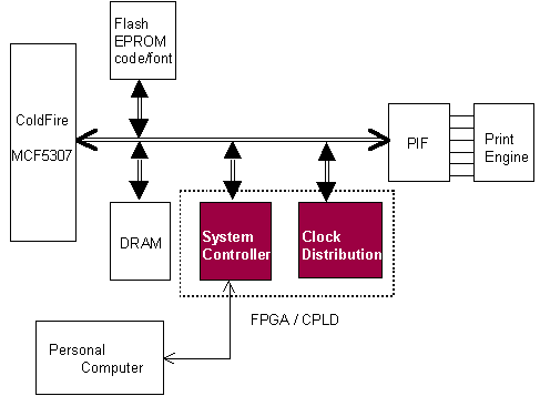
Figure 6: Adding PDL to the Printer Interface
The ColdFire is particularly complete for interfacing to external DRAM
and Flash EPROM modules. In Figure 6, the programmable
logic is relegated to completing the external interface, packing and unpacking
the address / data modules and distributing the clocks to the rest of the
system. As well, interface resolution to the PIF is handled by the
programmable logic. The processor deals with the font/code EPROM
as well as the larger DRAM memory modules which retain the encoded PDL
to be "cracked".
Adding RET and RIP
So what is Resolution Enhancement Technology (RET)? RET is a combination
of several techniques, and varies among manufacturers. For instance, large
dots can effectively cover paper, but fail to properly deliver adequate
visual resolution for detailed graphic images ö or even elaborate
text fonts. By increasing the number of dots and squeezing individual
dot sizes down, it is possible to improve the perceived quality of a produced
image. Frequently printer vendors refer to this as reducing the "jaggies".
Simply increasing the dots per inch is one strategy. Care must be
taken to assure that dot bleeding into the media does not negate the advantage
attained.
Figure 7 demonstrates this effect where the line drawn on the left models
600 dpi and the one on the right models 300 d.p.i. In particular,
observe the edges of the two lines ö the 300 d.p.i. line has an exaggerated
scallop or jagged effect compared to the one on the left. When delivering
the various edges and shapes, RET creates the edges with more dots of smaller
size. Naturally, this "technology" is basically lookup table RAM
or ROM blocks loaded with patterns that the design software uses to build
up sweeter edges.
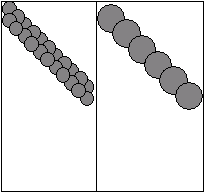
Figure 7: Reducing the "jaggies" with 2X dpi (left represents 600
dpi, right 300 dpi)
Figure 8 shows the effect of more advanced RET. Starting with the
image on the left side, a series of transformations occur that can produce
the image on the right, with greater visual appeal and clarity. To
start, the crosshatched circles are dots that have the fuzzy quality of
being "do not care" dots. It is unclear whether the dots should be
dark or light. By a set of heuristic choices and dot level operations
shown in the center blocks, a final result for what gets printed (without
the fuzziness) is delivered on the right. The process combines low
level DSP and heuristic choices.
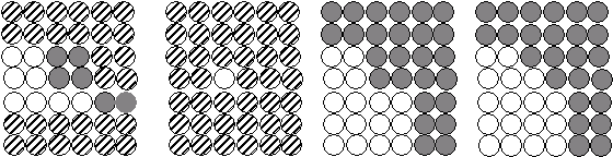
(a) initial image
(b) transformation 1 (c) transformation 2
(d) enhanced image
Figure 8: Image Enhancement Transformations
RET requires managing a set of memory structures and finding substitution
bit patterns with greater resolution. It is usually done with a microprocessor
and today's choice is frequently the ARM 7 RISC, which is frequently offered
as an ASIC standard block. Hence, with the combination of an ASIC,
a microcontroller and additional expense, it is appropriate to keep adding
capability. The current trend is to add Raster Image Processing (RIP),
as well.
RIP is usually the last stage in creating the delivered bitstream to
the print engine. RIP involves managing a page or band buffer which
holds the actual bitstream delivered to the engine. RIP is so similar
to video signal creation, that the RIP output is usually called video out.
Because page buffering is expensive (i.e., lots of DRAM), software that
can effectively create and juggle bit buffers while maintaining data flow
from the host are in high demand. Band memory buffering is the technique
of producing smaller strips of information delivered to the engine while
more data is being "RIPped". Figure 9 ties it all together.
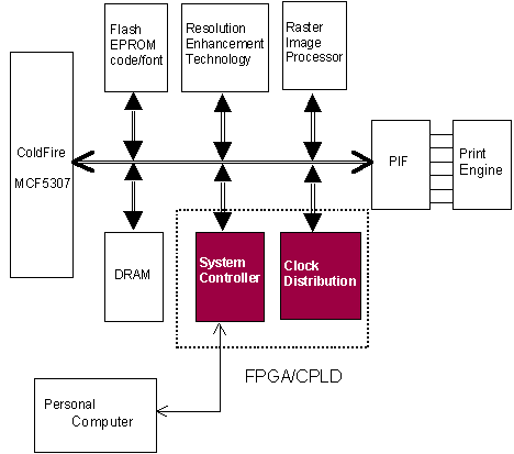
Figure 9: Adding RET and RIP to the basic structure
Note that the RET and RIP capabilities exist in ASSPs. One such device
is made by Conexant, called the MFC1000. The MFC1000 includes substantial
circuitry to actually build up a MultiFunction Peripheral, save the FAX
Modem circuitry. In this situation, a Spartan-II FPGA does the general
interfacing to the PC, the ColdFire, memories, the MFC1000 and the PIF,
as well as the usual LED driving and switch debouncing duties.
Going Beyond . . . MultiFunction Peripherals
Adding a microprocessor and memory to the ASSP, along with small amounts
of memory and additional timer circuits permits an elaborate extension
of the basic printer. There has been a frustration for some time
in Small Office/Home Office (SOHO) environments where the available deskspace
occupied by a laser printer, a FAX machine, a scanner and copier are dear.
Recognizing that these processes all either move transducers across paper,
or vice versa, it was noted that they have a lot in common. The MultiFunction
Peripheral (MFP) evolved to meet this need in a single package. Clearly,
there will be a tradeoff in that an MFP will not have every bell and whistle
that separate units have, but with today's quality being what it is, these
devices are irresistible. Currently priced in the mid-range
ink jet printer range (typically $400-500), these devices are "taking off".
Several MFP ASSP parts exist for completing the MFP picture. Letâs
expand on the Conexant solution using the MFC1000 and gluing the rest of
the system together with a Spartan FPGA.
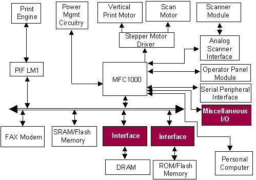
Figure 10: MultiFunction Peripheral Controller
In Figure 10, the Spartan-II FPGA interfaces the DRAM, the ROM/Flash Memory,
the Operator Panel Module, the Serial Peripheral, Miscellaneous I/O and
the PC. All these interfaces are very specific to the chosen devices (DRAMs,
ROMs, etc.). |