![]()
The Future of FPGAs
A white paper by the company that invented them
Introduction
As programmable logic suppliers accelerate their use of advanced deep submicron
technologies, digital designers can expect to see higher densities and
faster devices at lower voltages that will be more competitive than ever
with traditional ASICs. Within the next decade, Xilinx believes that programmable
logic will become one of the largest segments of the logic market, surpassing
both standard logic and masked gate arrays. This phenomenon will change
how logic is designed, making programmable logic pervasive in many engineering
organizations. This white paper examines a number of fundamental questions
about the changes taking place with high density programmable logic technology.
And it examines how Xilinx, as the inventor of FPGAs and the industry's
leading innovator, is providing answers to those questions.
FPGAs: The New Process Drivers
New field programmable gate arrays (FPGAs) manufactured using advanced
0.35 and 0.25 micron technology and offering in excess of 100,000 logic
gates will be widely available during 1997. In a shift that brings them
to the forefront of progress in semiconductor manufacturing, FPGAs today
are becoming ideal vehicles for driving CMOS process technology development.
It is easier to quickly identify manufacturing process defects in FPGAs,
which are standard SRAM-based devices, than it is in, say, microprocessors.
In addition, ever higher transistor counts in FPGAs and their use of multiple
metal interconnect layers truly stress a CMOS process. For example, the
new Xilinx XC4085XL FPGA, the industry's highest density device scheduled
for delivery during the first half of 1997, is fabricated on a 0.35 micron,
three-layer metal process. The XC4085XL has 16 million transistors, more
than three times the number in Intel's Pentium ProTM
processor. As Xilinx makes the transition to 0.25 micron, five-layer metal
technology in the near future, the company plans to manufacture parts with
more than 30 million transistors. Before the turn of the century, Xilinx
will be using 0.18 micron technology to build devices with 60 million transistors.
Using FPGAs as process drivers ensures that design engineers will have
access to the largest and fastest devices that can be built using any technology.
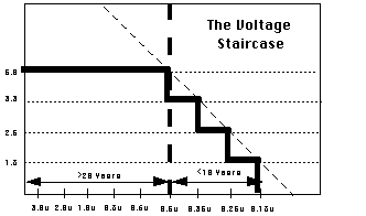
The Voltage Transition Ahead
These new, lower voltage products mark a major transition for FPGA users,
who have been designing exclusively in a world of 5V supply. Incorporating
0.35 micron FPGAs into new designs will require a 3.3V power supply voltage;
0.25 micron will mean a move to 2.5V. Further voltage migrations will be
required when 0.18 micron and finer geometry components reach the market.
This accelerated voltage migration is unprecedented. For more than twenty years 5V has been the standard supply voltage. The next step to 0.35 micron devices running at 3.3V, some observers believe, may well be the shortest-lived supply standard as products rapidly move down the "Voltage Staircase" to ever finer geometries and incrementally lower voltages.
Under the old model in the 5V-only world, engineers could expect predictable improvement in price and performance without having to change designs to accommodate smaller and faster versions of an FPGA (or any other semiconductor device). Over the past several years, as FPGAs moved down the process curve from 3.0 micron to 2.0 micron, then to 1.0, 0.8, 0.6 and finally 0.5 micron, die sizes shrank while remaining socket compatible and operating at 5V.
The Incentive to Migrate
Now, if digital designers want to enjoy the benefits of more speed and
lower cost in future generations of high density, high performance FPGAs,
they will have no choice but to migrate to lower voltage parts. This will
force the issue of ever-changing supply voltages into design and product
life-cycle assumptions. Although older technology devices will still be
available, they will not go through rapid price declines over time as they
have in the past. There will be an economic incentive to use newer-technology
devices, and design voltage and process migration capability into systems
to achieve cost savings over the life of a product.
How are engineering organizations planning for this upheaval? Xilinx recently surveyed more than 600 FPGA applications engineers and system designers worldwide on their current and future plans to migrate to lower voltages. Respondents were involved in a broad array of applications ranging from PCs and data communications to networking and imaging. The study generally concluded that while many designers moved to 3.3V FPGAs in the past because of power considerations, they are now making the move because the biggest, fastest and newest chips are only available in 3.3V. While some respondents see 3.3V usage on the rise, especially in the areas of DSPs, MPUs, SRAMs and DRAMs, they believe many 5V components--for example, D/A converters, UARTs, disk controllers and older peripheral chips--will remain in the picture for some time. Part of the reason for incomplete product offerings at 3.3V is the economics of device manufacturers.
Mixed Voltages: Rule Rather Than Exception
For products that do not have sufficiently high performance demands to
require the latest processes (which are limited to 3.3V or lower), it is
more economical for the device manufacturer to continue building that product
on a mature 5V process for which the processed wafers are much less expensive
than the latest 3V or 2.5V processes. But the increased die-per-wafer yield
of the new process technologies will quickly make products developed on
them more cost effective.
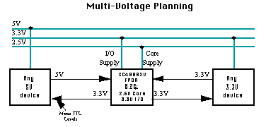
While most users would prefer to have a single power supply system, they recognize that mixed voltage systems will be the rule rather than the exception for the immediate future. How quickly users will move to lower voltages depends largely on individual objectives. Those who want the newest, fastest and biggest devices will be the first to convert to 3.3V.
The results of the Xilinx survey point to three major areas of concern: supply voltage, I/O interface standards and power.
Supply voltage: Respondents are planning to deal with mixed voltage systems in a variety of ways. It is already commonplace to see high performance microprocessors and memories with power supplies of 3.3V and 2.5V. This has caused a need for multi-supply boards. Some users plan on retaining their large 5V power supplies and using local DC/DC converters to supply lower voltage chips. Others are considering a move to much higher voltages (48V, for example) as the power distribution medium and using DC/DC converters for all power needs including 5V and lower voltages. The trend toward more usage of 3.3V and 2.5V devices in some areas, combined with the already noted intention of some component vendors not to rush toward conversion, will force users to deal with multi-voltage boards for some time to come. To deal with this situation, some customers are turning to programmable power supplies as part of the solution.
I/O interfaces: It is well recognized that I/O standards must also change as supply voltages drop. Xilinx, for example, has already designed 5V input tolerance into its new-generation 3.3V FPGAs. These new devices accept 5V signals on all I/Os and can drive TTL levels into any 5V device, eliminating any interface issues. Future devices will have multi-voltage I/Os capable of interfacing between a variety of I/O standards. This multi-standard interface capability becomes vital as FPGAs are used more and more as a system solution rather than just a logic component.
The situation today is that the familiar 5V TTL interface standard is being challenged by a variety of lower voltage standards. The 3.3V LVTTL standard is widely used, but many others have some use in focused niches such as the use of GTL interfaces for high performance processors.
There now exits a veritable alphabet soup of I/O standards, including LVTTL, GTL, GTL+, RSL, HSTL, SSTL, LVDS, PECL, to name a few. Another major concern is whether device manufacturers will be able to maintain 5V interface capability as they move from 3.3V to 2.5V processes. With the large number of 5V devices still being designed into systems, users would like to retain the ability to connect these older devices to devices using the latest technology, without incurring the added cost and performance degradation associated with translator devices.
Power is an issue as system integration increases. Power consumption increases as operating frequency increases. With larger devices the problem is amplified by the large number of transistors being switched. Users of large ASIC devices have been dealing with this problem by using advanced 3.3V (or lower) processes for their largest and highest performance designs. With the size of all ASIC devices, including FPGAs, growing rapidly, and with operating frequencies going up as well, attention to power has become extremely important for both device vendors and users.
In the design of its XC4000EX family of FPGAs, for example, Xilinx continued with its patented segmented interconnect architecture that prevents unnecessary interconnect capacitance from slowing down operation and causing extra power dissipation. In future generations of products, Xilinx will further extend this capability to ensure higher operating frequencies without power dissipation problems while maintaining greater system reliability.
New Density Metrics
As FPGAs offer more and more density, it becomes increasingly important
that customers be able to accurately differentiate competing products.
Ideally, FPGA capacity metrics should be an accurate indication of the
amount of logic that can be implemented within a given FPGA device. At
the same time, it should reflect the relative capacity of comparable devices
from competing manufacturers. But this ideal situation seldom occurs.
Most vendors, including Xilinx, have described device capacities in terms of "gate counts." That is, the number of 2-input NAND gates that would be required to implement the same functionality. This metric has the advantage of being familiar to ASIC designers. And in theory, it allows the comparison of programmable logic device capacities to those of traditional mask-programmed gate arrays.
However, FPGAs do not consist of 2-input NAND gates. They have structures such as look-up tables, multiplexers, three state buffers and flip flops for implementing logic functions. This makes counting gates an inexact science at best, and the problem is compounded when different vendors apply varying methodologies to determine their gate counts. All too often, gate counting becomes a game of "one-upsmanship" among programmable logic suppliers. As a result, comparing gate-count statistics supplied by different FPGA vendors can be misleading.
The majority of FPGAs in use today are SRAM-based FPGAs whose logic blocks are based on a combination of memory look-up tables (LUTs) and dedicated registers.
FPGA families with LUT-based logic blocks include the Xilinx XC3000, XC4000, and XC5000 families, the Altera FLEX families, and the Lucent Technologies ORCA families. Although differing architecturally in many other respects, the common use of LUTs and registers as the primary logic resource suggests a more direct and objective capacity metric than gate counts.
Xilinx is proposing a new methodology for measuring logic density based on "logic cells." A logic cell is defined as the combination of a 4-input look-up table and a dedicated register that reside in the same block, such that the output of the LUT can be the data input to the register.
Using this definition, the XC3000 FPGAs have 1.5 logic cells per CLB; the XC4000, 2.375 logic cells per CLB; the XC5000 and ORCA 2C FPGAs, 4 logic cells per array element; and the Altera FLEX FPGAs, 8 logic cells per array element. The following example demonstrates how logic cells is a more accurate measure to compare competitive products that have approximately the same logic density.
| Company |
Product |
Logic Cells |
Vendor's Gate Counts |
| Xilinx |
XC4028 |
2432 |
28,000 |
| Altera |
FLEX EPF10K40 |
2304 |
40,000 |
| Lucent |
ORCA 2C26 |
2304 |
26,000 |
Xilinx believes this new methodology will make it possible for customers to make meaningful comparisons of competing products and end the confusion that results when programmable logic vendors include on-chip RAM to arrive at inflated gate densities.
System Level Integration on High-density FPGAs
The unique flexibility and strong time-to-market attributes of FPGAs have
made them the preferred solution for many applications where standards
and end-user requirements are constantly changing. FPGAs have succeeded
in several fast emerging market segments such as wireless communication,
networking and multimedia applications. An FPGA traditionally has been
used to integrate the glue logic in a system. However, a significant change
in usage is taking place in the market. With rapidly growing densities
and performance, FPGAs are being used for System Level Integration (SLI),
that is, integration of very high-performance, high-density systems or
sub-systems, previously implemented in semi-custom ASICs.
When doing high-density, high-performance SLI designs, FPGA users face the same productivity challenges as the high-end ASIC users. The design complexity is growing while the time to market is shrinking. Old design methodologies are no longer good enough to complete those complex designs in the required time. The shift from schematic entry to HDL and synthesis has already taken place, and designers are now looking forward to the next generation of tools and design methodologies -- high level, pre-defined building blocks for FPGAs. This will allow designers to raise the abstraction level of the design and focus on the system design rather than the gate design.
FPGAs: The Mass Market for Cores
Providing cores is not new in the ASIC domain. Several gate array vendors
have been successful with core programs, winning key designs by providing
libraries of cores that customers use to complete a system design on a
chip. However, the ASIC vendors' core solutions have not been for everyone.
Doing a core-based design has traditionally required intensive technical
support. The business model for an IP provider in the ASIC world calls
working with a few, high revenue generating customers. For example, many
gate array vendors typically demand a $5-10 million opportunity before
they commit to a core-based design.
The FPGA market, on the other hand, has different demands. The great success of FPGAs is a result of benefits such as design flexibility, short development time, low initial cost and reduced risk. Designers who use FPGAs are accustomed to getting started with minimal cost and effort, and completing the design with little involvement from the FPGA vendor. The model for providing cores to the FPGA customer must not contradict those key benefits, but enhance them to make SLI on high-density FPGAs flexible, fast and cost effective. An intellectual property (IP) provider in the FPGA market cannot work only with a few big customers. Cores must be accessible for all customers, which means that cores must be easy to use and easy to acquire.
To maintain the time to market benefit, design requirements must be met without extensive optimization and verification of the core. Furthermore, the FPGA architecture (look-up tables, multiplexers and registers) is substantially different from a gate array architecture (sea of gates). As a result, cores must be well optimized to the targeted architecture to achieve the required performance and the best device utilization at the lowest cost.
Shrink-wrapped Cores
With its successful introduction of the LogiCore PCI interface--now in
use by hundreds of designers--Xilinx has identified three key requirements
that must be fulfilled to enable a designer to finish a core-based, high-density
FPGA design in a timely manner:
Quality: Cores must be fully verified and highly optimized for best device utilization.
Predictability: Cores must meet timing and functionality requirements without manual intervention.
Support: The right expertise must be available when problems arise.
By carefully optimizing a core to the target architecture, predefining the critical paths of the design, and extensively verifying a core before it is released, customers can achieve significant reduction in design time and risk. An FPGA user must be able to customize a selected core, plug it into the targeted design and know that timing and functionality are met. Engineering resources can then be focused at the system-level design and the unique functions that add value to the final end-product. This is especially important for high-performance functions such as a PCI interface, which pushes the FPGA technology (or any technology) close to the performance limit. If the implementation of critical paths is not pre-defined, timing will be affected by the selection of EDA tools and adjacent logic.
PCI as a design example
The LogiCore PCI interface is an excellent example of how designers can
benefit from a verified FPGA core. A customer who designs a PCI system
from scratch must first learn the details of the PCI standard, which is
a daunting and complex specification. Then comes the task of learning how
to implement the PCI Interface in the FPGA architecture to meet timing.
This effort may take days, weeks or months depending on previous experience
with PCI and FPGA designs. After learning the application, significant
time will be spent designing, implementing and tuning the design; this
is a tedious process that will take months even for an experienced design
engineer.
The last and most rigorous part of the design process is verification. The designer must create an extensive set of test vectors or buy a third-party test bench to verify the functionality. Again, PCI is an extremely complex design, and a customer should count on a couple of months for verification and debugging. A generic synthesizable core gives a good starting point for an FPGA design. But once the functional design is done, most of the implementation, tuning and verification must still be completed by the designer. This is a major task for a high-performance function such as PCI. Using the Xilinx LogiCore PCI Interface, however, where all critical paths are predefined, the designer can focus on the unique back-end functions of the design and other system-level trade-offs. Xilinx estimates that its LogiCore PCI Interface can save customers more than six months in development time.
Xilinx plans to continue introducing LogiCore products to support high density, high-performance designs. Xilinx has combined a strong internal core development team and an in-house application organization with a network of third-party IP providers. The company plans to offer its customers a growing portfolio of shrink-wrapped cores, including the LogiCore products which are sold and supported by Xilinx, and AllianceCore products, which are sold and supported by third-party vendors and optimized for Xilinx FPGAs. Future products will include faster and lower voltage versions of the PCI Interface, a USB device controller, DSP filters, correlators and multipliers, and basic blocks such as DMA controllers.
Xilinx HardWireTM Arrays
The Xilinx HardWire program will support new, higher density programmable
logic devices for customers who require a no-risk path to a mask programmable
solution in order to achieve the lowest possible cost. The Xilinx roadmap
includes fully compatible 3.3-volt HardWire devices in 1997 and 2.5-volt
HardWire devices in 1998. HardWire devices are guaranteed to be fully logic
and pin compatible with their FPGA counterparts at ASIC-like prices, and
they eliminate the need for customers to write test vectors or perform
exhaustive timing simulations. HardWire is the industry's only fully seamless
and compatible FPGA conversion service to reduce time-to-volume production
for today's rapidly shrinking product life cycles.
The Xilinx HardWire family FPGA-specific mask-programmable logic arrays are specially designed to support the functionality, features and performance of Xilinx field-programmable devices. For each standard XC4000EX FPGA device, there is an equivalent XH4000EX HardWire device. These devices are optimized for fast, DesignLock conversion from the customer-verified FPGA database.
Xilinx guarantees fast conversion from a customer FPGA design to an equivalent HardWire Array through the patented DesignLock Conversion Process, which preserves all characteristics and features of the original FPGA design. This conversion is turn-key, automatically mapped and verified by Xilinx, based upon the customer-verified FPGA design.
HardWire also supports all unique functions and features of Xilinx FPGAs such as I/O characteristics, power-on reset, configuration modes, JTAG and RAM/ROM.
Xilinx delivers prototype devices in as little as four to six weeks, depending on customer design complexity and required features, in the qualified production package and process. During 1997 Xilinx plans to further reduce prototype delivery times. Such rapid conversion can be accomplished without exhaustive simulation and verification because the DesignLock conversion process uses the customer's design, which has already been verified and implemented successfully in the FPGA.
Conclusion
Clearly, digital designers face their share of challenges ahead as they
attempt to fully understand the newest wave of deep submicron FPGAs and
related solutions and incorporate them into their next generation of products.
During this transition period, Xilinx is committed to working closely with
its customers to ensure that they can harness the increased performance,
lower power and cost improvements of these exciting FPGA products.