|
||
|
|
||
Xilinx : Support : techXclusives |
|||||||||||||||||||||||||||||||
|
|
|||||||||||||||||||||||||||||||
| techXclusives | |||||||||||||||||||||||||||||||
|
|||||||||||||||||||||||||||||||
|
|||||||||||||||||||||||||||||||
|
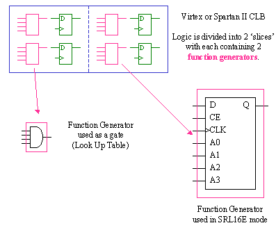
INTRODUCTION LEVEL: The SRL16E was introduced with the Virtex architecture and has been included in all Virtex variants and the Spartan II devices. Although it sounds like an additional component, it is in fact an alternative mode of operation for every function generator (look up table) which are part of every CLB. Use of this exciting mode can rapidly lead to cost saving of an order of magnitude. Although there are cases where the SRL16E may be used automatically to save silicon area, the SRL16E will appear most in designs that have been well engineered. This Tech� Topic is intended to empower you, the engineer, to see ways in which you can exploit this feature and dramatically improve your design with associated lower costs.
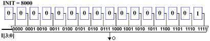
Clearly, the SRL16E mode looks very much more complex --and indeed, it needs to be to bring such dramatic cost savings to a design. However, the operation of this mode is not obvious, and an understanding of the underlying structure of a function generator is very helpful in helping you to exploit it. Consider the following model for a function generator used as a look-up table. The 4 input signals I3, I2, I1, and I0 are used as the select lines on a 16 to 1 multiplexer. The data inputs to the multiplexer are the 16 configuration bits, which are set via the configuration bit-stream. In this example, a 4-input AND gate is shown. Only when all 4 multiplexer select lines I[3:0] are high is the configuration cell containing logic �1� selected. In all other cases, the multiplexer will select a logic �0.� The INIT parameter is a description of the bit pattern stored in the configuration cells. This hexadecimal value representing the bit pattern 1000 0000 0000 0000 can be applied manually to a lookup table primitive (LUT4 component), or is more normally generated automatically from a schematic of HDL synthesis package.
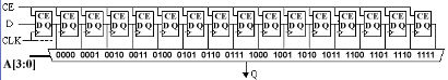
When the function generator is used in SRL16E mode, the basic structure is the same. The 4 inputs which act as select lines to the multiplexer have now been called A3, A2, A1, and A0, but their ability to select one of 16 inputs remains the same. The major difference is that the 16 configuration cells have now been organised as a shift register. As well as being able to initialise these cells via the configuration bit-stream in the same way as the lookup table (using an INIT value), the contents can now be modified by shifting in new data from within the design itself.
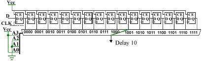
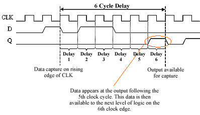
The output has been called "Q" to reflect that it is the result of selecting a "Q" output of one of the flip-flops in the shift register. Note that although the shift register is provided with a clock and clock enable, the ability to select different flip-flops by changing the A[3:0] inputs is independent of the clock in just the same way as the lookup table. BASE LEVEL: The most direct application of the SRL16E is in the implementation of digital delay or shift registers. Consider an example where 10 clock cycles of delay are required on a signal for which the circuit would consist of 10 simple flip-flops...
This function would normally be associated with the use of 10 individual flip-flops, and would therefore occupy 5 "slices" (2� CLBs) of the Virtex/Spartan architecture. Using the SRL16E enables this function to be replaced by just one function generator. The application of appropriate logic "0" and logic "1" controls is all that is required to set the length of delay. In this example, the shift register is permanently enabled; hence, the CE input is also tied high.
In order to select the 10th flip-flop of the SRL16E shift register, the multiplexer must be forced to use the "1001" data input. It can be confusing as this is the value 9, but is actually the same as the way we label a bus starting with bit 0 and the 10th wire as bit 9. It is obvious that a function generator can be connected to support a delay from 1 to 16 clock cycles. Less obvious is that high performance is now much easier to achieve in a system design. Since all the flip-flops are now fixed in the silicon, the connections between them are very short and predictable. The lower utilisation of the device also enables other logic to be placed in closer proximity. Although Vcc and GND signals must be routed to the SRL16E, these are static signals which have no impact on timing or power consumption. Ultimately, each CLB now contains 68 flip-flops ( 4 x [16+1] ), which greatly increases the potential gate count of the device. The 96 CLBs of a XC2S15 (the 15,000 gate Spartan device) could implement 6528 bits of shift register. This is the equivalent of over 39,000 ASIC gates (without even considering the 16k bit of block RAM also on the device). -- Use of the SRL16E in the delay configuration is relatively simple. Being aware of when it can be used is vital in ensuring maximum utilisation of a device. This is particularly true when using an HDL synthesis tool. Believe it or not, you may already have used this powerful feature of the device because most synthesis tools will automatically insert SRL16E into your design to replace multi-stage delays. The issue is that failure to use the SRL16E either manually or automatically will have a large impact on the area of silicon occupied. The following points are worth considering when designing with any tool: 1. No Reset - 2. Simulation Confusion -
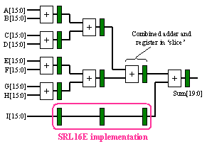
-- Consider some applications in which shift register delay can be used, or indeed occurs by default: 1. Pipeline Compensation - For high performance designs, Virtex and Spartan provide excellent results when fully pipelined. Unlike an ASIC, the flip-flops in each CLB "slice" are already provided and waiting to be used. Although the pipeline registers are in themselves free, a pipelined system may have additional cost caused by pipeline compensation of other paths.
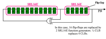
This example shows the addition of 9 values of 16-bits. It can be seen that the 9th input has to be delayed by 3 cycles to compensate for the addition tree of the other 8 inputs. This compensation delay requires 48 flip-flops (3?16) which would occupy 12 CLBs. The SRL16E�s reduce this to just 16 function generators in 4 CLBs. 2. Pseudo Random Noise Generator - A pseudo random noise generator is based on a Linear Feedback Shift Register (LFSR) counter technique. There are actually a couple of different styles of implementation, but both make use of simple shift register delay. The PN generator is responsible for producing a signal that "randomly produces logic "0" and logic "1" levels.
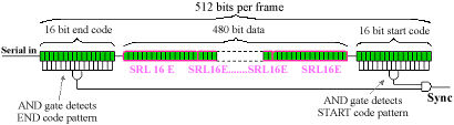
Note that a pseudo random "number" generator is the same structure, but would observe all bits of the shift register as a parallel word. This would not enable the SRL16E�s to be used other than to provide single flip-flops and obtain 8 flip-flops per CLB. -- In some applications the realisation that the SRL16E can provide such efficient shift register delays can be utilised to greatly simplify designs. This is explored more later, but first a direct application seen regularly: Serial Frame Synchronizer - This is actually a common application seen in telecommunications and networks. Data is passed serially between units (say at 2.048Mbit/s) and has been formatted into frames or packets. In order to synchronize to these packets, a start code is included. Although this code is considered to be relatively unique, there is always the possibility that the data itself may contain the same pattern. To greatly reduce the probability of incorrect synchronization, an end of frame code can also be applied. Only when the start code and end code occur at the correct times is the data accepted. The state machine approach to this design problem is to look for a start code and then begin storing data in a buffer. It would then check for the end of frame code at the appropriate time. If the stop code does not occur when expected, or if a start code occurs beforehand, then the buffer is overwritten with new data. Since this has the possibility of loosing data, the design of the state machine and data buffers can become very complex, but never perfect.
The ideal solution is simply to hold an entire frame in a shift register and test for the start and end patterns at every bit position. Shown above is a 512 bit frame detector. As each new bit is received, the whole shift register advances by one position. AND gates connected to flip-flop based shift registers are able to detect the simultaneous occurrence of the 16 bit start and end codes. The separation of start and end codes is then achieved by a simple shift register delay of 480 bits requiring 480 flip-flops. This 480 flip-flops would normally occupy 120 Virtex/Spartan CLBs and would be considered expensive. Using the SRL16E mode reduces this 480 bit shift register to 30 function generators in 7� CLBs. In this way the entire (perfect) synchronizer can be realised in just 15� CLBs. An equivalent gate count of over 3000 achieved in 16% of the Spartan 2S15 (15,000 gate device). Share your comments, questions and ideas with Ken Chapman and other interested designers at the "SRL16E" FORUM. |
|||||||||||||||||||||||||||||||
| |
|||||||||||||||||||||||||||||||
|
|||||
|
|
Troubleshoot | Hardware
| Software | Library
| Design | Education
| Services | | Home | Products | Support | Education | Purchase | Contact | Search | |