|
 |
|
|
More specific to the matter at hand is the design of manufacturable artifacts. This activity uses all facets of design because, in addition to the specification of a producible object, it requires the planning of that object's manufacture, and much problem solving along the way. Design of objects usually begins with a rough sketch that is refined by adding precise dimensions. The final plan must not only specify exact sizes, but also include a scheme for ordering the steps of production. Additional considerations depend on the production environment; for example, whether one or ten million will be made, and how precisely the manufacturing environment can be controlled.
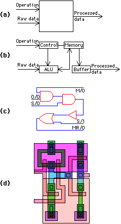
| This book is particularly concerned with the design of highly complex electronic circuits, referred to as VLSI (very-large-scale integrated) circuits. When doing design of VLSI systems, the same steps must be taken (see Fig. 1.1). An initial sketch shows the "black box" characteristics of a circuit: which wires will bring what information and which wires will get results. This is then refined into an architectural design that shows the major functional units of the circuit and how they interact. Each unit is then designed at a more detailed but still abstract level, typically using logic gates that perform inversion, conjunction, and disjunction. The final refinement converts this schematic specification into an integrated-circuit layout in whatever semiconductor technology will be used to build the chip. It is also possible to produce working circuits without the need for custom chip fabrication, simply by assembling standard chips to perform the specified function. Although design rarely proceeds strictly from the abstract to the specific, the refinement notion is useful in describing any design process. In actuality, design proceeds at many levels, moving back and forth to refine details and concepts, and their interfaces. |
|
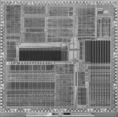
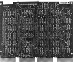
A semiconductor process technology is a method by which working circuits can be manufactured from designed specifications. There are many such technologies, each of which creates a different environment or style of design. In integrated-circuit (IC) design, which is the primary focus of this book, the specification consists of polygons of conducting and semiconducting material that will be layered on top of each other to produce a working chip (see Fig. 1.2). When a chip is custom-designed for a specific use, it is called an application-specific integrated circuit (ASIC). Printed-circuit (PC) design also results in precise positions of conducting materials as they will appear on a circuit board; in addition, PC design aggregates the bulk of the electronic activity into standard IC packages, the position and interconnection of which are essential to the final circuit (see Fig. 1.3). Printed circuitry may be easier to debug than integrated circuitry is, but it is slower, less compact, more expensive, and unable to take advantage of specialized silicon layout structures that make VLSI systems so attractive [Mead and Conway]. Wire-wrap boards are like printed-circuit boards in that they use packages that must be precisely positioned. However, they allow the wire locations to fall anywhere as long as they connect to the posts of the IC packages. Such boards are typically manufactured as prototypes for less expensive PC boards.
|
|
The design of these electronic circuits can be achieved at many different refinement levels from the most detailed layout to the most abstract architectures. Given the complexity that is demanded at all levels, computers are increasingly used to aid this design at each step. It is no longer reasonable to use manual design techniques, in which each layer is hand etched or composed by laying tape on film. Thus the term computer-aided design or CAD is a most accurate description of this modern way and seems more broad in its scope than the recently popular term computer-aided engineering (CAE). Although CAE implies a greater emphasis on circuit analysis, the term has instead been used to describe the recent spate of design systems that are attractively packaged on workstations. These systems all seek to aid in the design of circuitry.
There are many steps that a computer can take in the design of electronic circuits. Graphical drawing programs are used to sketch the circuits on a display screen, whereas hardware-description languages achieve the same result textually, employing the expressive power of programming languages (see Fig. 1.4). Special synthesis programs convert among the different refinement levels of a design, and analysis programs help to check circuit correctness. A final step converts the design to a manufacturing specification so that the circuit can be fabricated. Thus computer programming is used throughout the circuit design process both as an aid to, and as a metaphor of, the design activity. In fact, the parallels between programming and VLSI design are very compelling and will be seen frequently in this book.
SYM mem
{
    DEF load %y load1, load2;
    TRAN (3,2) %270 t3, %270 t4, %270 t5, %270 t6;
    TRAN (12,2) t1, t2;
    DEF metaldiffusion md1, md2, md3, md4;
    DEF polydiffusion pd1, pd2, pd3;
    DEF metalpoly mp1, mp2, mp3, mp4;
    IDEF DIFF d1, d2, d3, d4, d5;
    IDEF METAL vi, vo S=vdd, gi, go S=gnd;

    # run power and ground
    W=4 vo RIGHT TO md1.m RIGHT 10 TO md2.m RIGHT TO vi;
    W=4 go RIGHT TO md3.m RIGHT TO md4.m RIGHT TO gi;

    # run pull-up 1
    md1.d DOWN 1 TO load1.v;
    load1.pp DOWN 8 TO pd1.p DOWN 7 LEFT 5 DOWN 3 LEFT 6 DOWN 9 RIGHT 0 TO t1.gw;
    pd1.d RIGHT 4 DOWN 8 RIGHT 4 DOWN 5 RIGHT 5 TO d4;
    d4 BELOW BY 1 t2.dn;
    t1.ds DOWN 2 TO md3.d;

    # run pull-up 2
    md2.d DOWN 1 TO load2.v;
    load2.pp DOWN 8 TO pd2.p DOWN 4 RIGHT 2 DOWN 6 RIGHT 9 DOWN 5 LEFT 0 TO t2.ge;
    t2.gw LEFT 0 UP 1 LEFT 4 TO pd3.p;
    pd3.d DOWN 2 LEFT 4 TO t1.dn;
    t2.ds DOWN 6 TO md4.d;

    # connect data lines
    t3.ds LEFT 4 TO d1 DOWN 9 TO d5 RIGHT 1 TO t5.ds;
    t4.dn RIGHT 4 TO d2 DOWN 9 TO d3 LEFT 1 TO t6.dn;
    t3.dn DOWN 0.5 RIGHT 4 TO load1.d;
    t5.dn UP 0.5 RIGHT 7 TO pd1.d;
    t4.ds DOWN 0.5 LEFT 4 TO load2.d;
    t6.ds UP 0.5 LEFT 7 TO pd2.d;

    # connect the select lines
    mp1.m RIGHT TO mp2.m;
    mp3.m RIGHT TO mp4.m;
    mp1.p DOWN 1 TO t3.gw;
    mp2.p DOWN 1 TO t4.gw;
    mp3.p UP 1 TO t5.ge;
    mp4.p UP 1 TO t6.ge;
}
|
| FIGURE 1.4 Hardware-description language for an nMOS memory cell. Initial code defines symbols (loads, transistors, contacts, points). Bulk of the code runs wires between components, implicitly placing everything. |
A fundamental assumption about VLSI circuits is that they are designed by humans and built by machines. Thus all CAD systems act as translators between the two. On one end of a CAD system is the human interface that must be intelligent enough to communicate in a manner that is intuitive to the designer. On the other end is a generator of specifications that can be used to manufacture a circuit. In between are the many programming and design tools that are necessary in the production of a VLSI system.
The front end of a CAD system is the human interface and there are two basic ways that it can operate: graphically or textually. Graphic design allows the display of a circuit to be manipulated interactively, usually with a pointing device. Textual design allows a textual description, written in a hardware-description language, to be manipulated with a keyboard and a text editor. For example, suppose a designer wants to specify the layout of a transistor that is coupled to a terminal. This can be done graphically by first pointing on the display to the desired location for the transistor and issuing a "create" command. A similar operation will create the terminal. Finally, the connecting wire can be placed by tracing its intended path on the display. To do this same operation textually, the following might be typed:
    transistor at (53,100).
    terminal below transistor by 30, left by 3 or more.
    wire from transistor left then down to terminal.
Notice that the textual description need not be completely specific
("left by 3 or more").
This is one of the advantages of textual descriptions:
the ability to underspecify and let the computer fill in the detail.
In this example, other parts of the circuit and other spacing rules will
help to determine the exact location of these components.
Additional advantages of text are the ease of verbal documentation, ease of
parameterization, ease of moving the CAD system between computers,
and a somewhat lower cost of a design workstation because of the reduced
need for graphics display.
The disadvantage of text, however, is immediately clear: It is not as good a representation of the final circuit, because it does not visually capture the spatial organization. Text is one-dimensional and graphics is two-dimensional. Also, graphics provides faster and clearer feedback during design, so it is easier to learn and to use, which results in more productivity. Although graphics cannot handle verbal documentation as well, it does provide instant visual documentation, which can be more valuable. Even underspecified spacing can be achieved graphically by creating an abstract design that is subsequently fleshed out.
A number of design styles exist to bridge the gap between text and graphics. These attempt to be less demanding than are precise polygon drawing systems while still capturing the graphical flavor. In sticks design [Williams], the circuit is drawn on a display, but the components have no true dimensions and their spacing is similarly inaccurate. Virtual grid design [Weste] also abstracts the graphics of a circuit, but it uses quasi-real component sizes to give something of the feel for the final layout. Closer to text is the SLIC design style [Gibson and Nance], which uses special characters in a text file to specify layout. For example, an "X" indicates a transistor and a "|" is used for metal wires, so the adjacency of these two characters indicates a connection.
| At the back end of a design system is a facility for writing manufacturing specifications. Complex circuits cannot be built by hand, so these specifications are generally used as input to other programs in machines that control the fabrication process. There are many manufacturing devices (photoplotters, wafer etchers, and so on) and each has its own format. Although standardization is constantly proposed there continue to be many output formats that a CAD system must provide. Figure 1.5 shows the structure of a simple CAD system with its front end and back end in place |
|
|
|
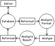
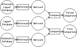
Between the front-end user interface and the back-end manufacturing specification are the analysis and synthesis tools that help reduce the tedium of creating correct layout. Analysis tools are able to detect local layout errors such as design-rule violations, and more global design errors such as logical failures, short-circuits, and power inadequacies. Figure 1.6 illustrates the sequence of analysis steps in a typical design system. Analysis tools can also be used to compare different versions or different views of the same circuit that have been independently designed (see Fig. 1.7).
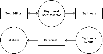
| Synthesis tools help perform repetitious layout such as programmable logic array (PLA) generation, complex layout such as routing, and even layout manipulation such as compaction. Figure 1.8 illustrates the sequence of steps for a typical synthesis tool. As circuit design becomes more complex, these tools become more valuable and numerous. |
|
Today's VLSI designers guide their circuit through the many different phases of the process outlined here. They must correctly control the initial creation of a design, the synthesis of additional detail, the analysis of the entire circuit, and the circuit's preparation for manufacturing. As synthesis tools become more reliable and complete, the need for analysis tools will lessen. Ultimately, the entire process will be automated, so that a system can translate directly from behavioral requirements to manufacturing specifications. This is the goal of silicon compilers, which can currently do such translation only in limited contexts by automatically invoking the necessary tools (see Fig. 1.9).
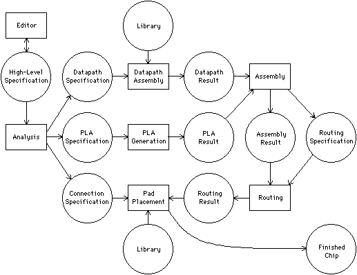 |
| FIGURE 1.9 Structure of a typical silicon compiler. |
Of course, totally automated design has been sought for as long as there have been circuits to fabricate. Although today's systems can easily produce yesterday's circuits, new fabrication possibilities always seem to keep design capability behind production capability. Therefore it is unreasonable to expect complete automation, and a more realistic approach to CAD acknowledges the need for human guidance of the design process.
The number of different computers continues to grow with each passing year. Although it would be foolish to recommend any particular machines for design use, certain requirements are clear and should be mentioned. In particular, large address space, good graphics, and effective communication are desirable features.
Large designs consume large amounts of memory. Whether that memory is primary or on a disk, it must still be addressed. Therefore design workstations should have the capability for addressing many millions of bytes at once. This means that 16-bit computers are inadequate and even 24 bits of addressing will not be sufficient. Many modern machines have 32 bits of addressing, which should satisfy designers for a few more years. Nevertheless, a truly forward-looking machine must have 36 or 40 bits of addressing to prevent the agony of inadequacy.
Graphic displays are becoming an integral part of many computer workstations. Although not every designer wants such a facility, it must be available at some point in the manufacturing of circuits. Color graphics is also important in VLSI design. Chapter 9, Graphics, discusses the many different display types and their relative merits.
As computers get smaller and less expensive, people buy more of them than ever before. Thus the modern design computer does not stand alone in its laboratory and must be able to communicate with the other workstations. Designers need to exchange circuit data and even need to switch computers when one fails or is busy. Thus sophisticated communication facilities are demanded to create a feeling that everyone is using the same computer. Also, human-level communications such as electronic mail must be supported.
One step toward a unified solution to CAD is a look at the decision processes required of a designer. The goal of design is to produce precise specifications that will result in a product that fulfills its intended purpose. To achieve this goal, the designer must weave through the myriad alternatives at each step. Should the object be taller or wider? Need the corners be rounded? Should this wire run under or over the board? These sorts of decisions must be made constantly and their answers depend on the particular requirements of the design. The object should be wider because that gives it more stability. The corners should be rounded because they can be fabricated with fewer errors. The wire should run under the board because it will obstruct components if it runs on top. Such collected information forms a set of constraints on the design, examples of which are shown in Fig. 1.10.
| ||||||||||||||||||||||||||||||||
| FIGURE 1.10 Design constraints. | ||||||||||||||||||||||||||||||||
Some constraints are inflexible and known to the designer before design begins. These constraints are the generic rules for design of a particular kind of object. For example, a logic designer may begin with the constraint of using strictly AND, OR, and NOT gates to build a circuit. More complex objects must all reduce to these at some point. Other prior knowledge is more subtle and is sometimes taken for granted, such as the constraint of having to do logic design with only two-valued logic (true or false) rather than multivalued logic or continuous (analog) logic. All of these are guiding factors to a designer.
Other design constraints are specific to the individual circuit being designed. Examples of these constraints are the particular components selected for the design, the location of power and ground paths, and the timing specifications. As design proceeds, the number of constraints increases. A good design leaves sufficient options available in the final stages so that corrections and improvements can be made at that point. A poor design can leave the designer "painted into a corner" such that the final stages become more and more difficult, even impossible to accomplish.
The hardest design constraints to satisfy are those that are continuous in their tradeoff and, because they compete with others, have no optimum solutions. An example of such constraints is the simultaneous desire to keep space low, power consumption low, and performance high. In general, these three criteria cannot all be optimized at once because they are at cross-purposes to each other. The designer must choose a scheme that meets specified needs in some areas and is not too wasteful in the others. The rules for this are complex, intertwined, and imprecise.
Given that design can be viewed as constraint optimization, one might expect that a circuit could be specified as a set of constraint rules that a computer could automatically solve. The result would be the best possible design, given the constraints. Although this can be done for very simple circuits, modern VLSI systems have so many constraints that no existing automatic technique can optimize them all. Also, many of these constraints are difficult for a computer to represent and for a human to specify. Simple design constraints that can be managed automatically have been the primary function of CAD tools, as the name suggests. These simple checks are very useful, because humans constantly lose track of the details and make flagrant design-constraint violations.
Computers do not lose track of detail, but they do have a more limited capacity than do humans to perform complex reasoning about nonspecific constraints. Recently, there have been attempts to mimic human design methods with the use of heuristics. These are imprecise rules that guide complex processes in ways that model human thought. Heuristics do not guarantee an optimal design; rather, they acknowledge the impossibility of considering every alternative and instead do the best they can. These rules plan the direction of design, eliminate many constraints as too insignificant to consider, and prioritize the remaining constraints to obtain a reasonably good result. This modeling of the human design process is part of the realm of artificial intelligence.
Regardless of whether a human or a machine does design, the endeavor is certainly one of constraint satisfaction. A good design system should therefore allow constraints to be specified, both as an aid to the human and as a way of directly controlling the design process. This enables CAD systems to evolve beyond the level of dumb sketchpads and fulfill their name by aiding in the design activity.
To understand VLSI CAD properly it is first necessary to discuss the characteristics of design in general and those of digital electronic design in particular. Two characteristics are universal to all design: the use of structural hierarchy to control detail and the use of differing views to abstract a design usefully. Two other characteristics are more specific to electronics: the emphasis on connectivity and the use of "flat" geometry in circuit layout.
Structural hierarchy views an object as parts composed of subparts in a recursive manner. For example, a radio may have hundreds of parts in it, but they are more easily viewed when divided into groups such as the tuner, amplifier, power supply, and speaker. Each group can then be viewed in subgroups; for example, by dividing the amplifier into its first stage and its second stage. The bottom of the structural hierarchy is reached when all the parts are basic physical components such as transistors, resistors, and capacitors. This hierarchical composition enables a designer to visualize an entire related aspect of some object without the confusing detail of subparts and without the unrelated generality of superparts. For example, the hierarchical view of an automobile fuel-supply system is best visualized without the distracting detail of the inner workings of the fuel pump and also without the unrelated generality of the car's acceleration requirements and maximum speed. Hierarchical organization is the most important characteristic in the design of any moderately complex object.
Another common technique is the use of multiple views to provide differing perspectives. Each view contains an abstraction of the essential artifact, which is useful in aggregating only the information relevant to a particular facet of the design. A VLSI circuit can be viewed physically as a collection of polygons on different layers of a chip, structurally as a collection of logic gates, or behaviorally as a set of operational restrictions in a hardware-description language. It is useful to be able to flip among these views when building a circuit because each has its own merit in aiding design. Designers of mechanical objects must also make use of multiple views so that the object can be understood completely. It is not sufficient to design a house solely with a set of floor-plans because that is only one way to express the information. Different views include the plumbing plan, perspective sketches showing solar exposure, and even parts lists that describe the house as comprising various quantities of wood, metal, and glass. Although different views can often be derived from each other in straightforward ways, they are useful to consider separately because they each cater to a different way of thinking and thus provide a "double check" for the designer.
More specific to VLSI design is the notion of connectivity. All electronic components have wires coming out of them to connect to other components. Every component is therefore interconnected with all other components through some path. The collection of paths through a circuit is its topology. This use of connectivity is not always present in mechanical artifacts such as planes or houses, which have optional connectivity and often contain unrelated components. However, there are other design disciplines that do use connectivity, in particular those that relate to flow between components. Thus plumbing, meteorology, and anatomy do make use of connectivity for their design.
The final characteristic of design is its particular geometric nature. All design disciplines have a spatial dimensionality in which they are significant. Automobiles have three dimensions; atomic structures and choreography have four because they are studied over time; music has one dimension to its presentation with an additional pseudodimension of the different notes; and physical VLSI design consists of two-dimensional layers that are placed on top of each other. An understanding of this dimensionality can be used to advantage when building design tools.
The rest of this chapter discusses these four aspects of design and introduces the necessary concepts for the constructions of VLSI CAD systems.
|
Previous |  |
Table of Contents | Next | |
Static Free Software |  |