 |
 |
|
|
| The third distinguishing characteristic of design, and the first one specific to electronics, is connectivity. Since electronics involves the movement of charge, components are all viewed in terms of how they move signals back and forth across wires. All components have locations that attach to wires that make a connection to other such locations on other components. Thus an implicit constraint of VLSI design is that everything is connected and the connections carry information about the relationship of the components (see Fig. 1.23). This suggests that networks are well suited to the representation of circuits. Networks are merely collections of nodes that are connected with arcs. For many VLSI design systems, the nodes of the network are components and the arcs of the network are connecting wires. Some systems reverse this to view signal values on wires as network nodes and the signal-changing components as network arcs. Yet another variation is to view both wires and components as nodes, with network arcs used to indicate connectivity [Ebeling and Zajicek]. Regardless of the way in which it is implemented, the network is a useful representation of circuitry. |
|
| In general, connectivity finds less use outside of circuit design. The representation of most physical objects is done with a combination of volumes, polygons, and other spatial objects. These have no inputs or outputs and therefore do not connect. But if the representation of physical structure has no need for connectivity, physical behavior often does. Fluid-flow design is a classic example of mechanical connectivity. In fact, fluid models are often used to explain circuit connectivity and behavior (see Fig. 1.24). |
|
| Many IC design systems work without any explicit mention of connectivity. The layout is created in a painting style that describes a circuit only with polygons that have no electrical connections. When two polygons adjoin or overlap, they are presumed to connect (see Fig. 1.25). In these design environments, the system must derive the connections from the nature of the polygon overlap. This difficult and time-consuming operation is called node extraction. The step is necessary in order to simulate or to statically analyze an integrated circuit. It can also be used to ensure that the layout geometry does indeed connect where it should and is not short-circuited. Given the fact that geometry-based IC design systems are ignorant about connectivity, the node-extraction step is quite important. |
|
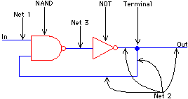
In most schematic design systems and some IC design systems, connectivity is essential to layout. Components must be wired together to form a completely connected circuit. An important concept is that of a net, which is a single electrical path in a circuit that has the same value at all of its points. Any collection of wires that carries the same signal between components is a net. If the components allow the signal to pass through unaltered (as in the case of a terminal), then the net continues on subsequently connected wires. If, however, the component modifies the signal (as in the case of a transistor or a logic gate), then the net terminates at that component and a new net begins on the other side.
| Figure 1.26 illustrates the notion of nets. There are three components shown in the figure: two active ones, which modify signals, and one passive one, which does not. The active components are the NAND gate on the left, and the NOT gate in the middle. The passive component is the terminal connection on the right (the blob). The figure also contains three nets. Two of them have been given labels: In and Out. The third net is an internal net that has no name. This unnamed net connects the output of the NAND to the input of the NOT gate. Notice that the Out net extends from the output of the NOT gate all the way back to the input of the NAND gate. |
|
The notion of a net is important in many steps of design, analysis, and fabrication. Designers often want to see an entire net so that they can see the path of a given signal. This path will then identify the origin of the signal and those components that use the signal as an input. Although some design styles mandate that only one component may output to a net, there are many in which multiple components may output to a single net. In some cases, the multiple outputs combine logically to produce a composite net signal (called a wired-or or a wired-and, depending on how the sources combine). In other cases, the circuit timing is planned so that only one component will output to the net at any given time, and the other components will have inactive outputs. The ability to visualize a circuit by nets is therefore important in understanding the paths between components.
Nets are also used in simulation because, viewed abstractly, a circuit is merely a collection of gating components and their connections. A list of nets (called a netlist) ignores the passive components and the actual geometry of the circuit layout. Therefore, if the simulator is concerned not with exact timing but only with the general functionality, then the collection of nets and active components is the only information that the simulator needs. Such simulators run faster than do those that consider timing and layout.
Circuit connectivity must be handled properly in the presence of hierarchy. When a cell instance is placed in a circuit, its contents must be able to connect to other components surrounding that instance. There are two ways to connect cell instances, depending on how they are placed. When the instances abut directly, they are linked by composition rules determined entirely by the location of wires inside of the cells. Conversely, when instances are separated by a channel that contains interconnecting wires, they are linked by connection rules specified by the layout outside of the instances.
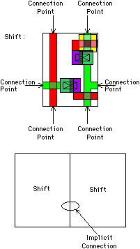
| There are two ways to implement composition rules: implicitly and explicitly. In those IC design environments that support only geometry and no explicit connectivity, hierarchical connections are made implicitly by ensuring that the layout in the cell definition connects spatially with objects at higher levels of the hierarchy (see Fig. 1.27). This raises the problem of accurate connection alignment, which is difficult to check automatically when there are no declared connection sites. However, most VLSI design systems understand the notion of an explicit connection point that is declared in a cell definition and is then available for use on instances of the cell at higher levels of the hierarchy (as in Fig. 1.11). This style of connection is similar to the notion of subroutine parameters in programming languages because the scope applies to the immediate higher level of hierarchy only. As mentioned before, the parallels between VLSI design and programming are significant and are seen frequently. |
|
Another important use of connectivity is in the programming of design constraints. Many constraints specify relationships among objects, so it is convenient to implement these constraints as special components that are connected into the circuit. As an example, suppose that a designer wishes to connect two transistors in a layout and to ensure that these transistors always stay on the same horizontal level. Figure 1.28(a) illustrates this layout using two MOS transistors and a connecting wire. In addition to the layout components and their connectivity, this figure shows an additional component: a constraint called "horizontal." It is connected to the transistors in much the same way that the transistors are connected to each other, the only difference being that the transistors are connected with a diffusion wire and the constraint is connected with a "constraining" wire. Thus the figure shows three components (two transistors and a constraint) and three connections (two constraints and a wire).
The contents of the constraint are shown in Fig. 1.28(b). The elements of this "layout" access data values, make decisions, and take actions concerning the updating of data values. It is the connection of this constraint to the layout in Fig. 1.28(a) that enables its contents to access and manipulate that design. More detail of this style of constraint specification will be given in Chapter 8, Programmability.
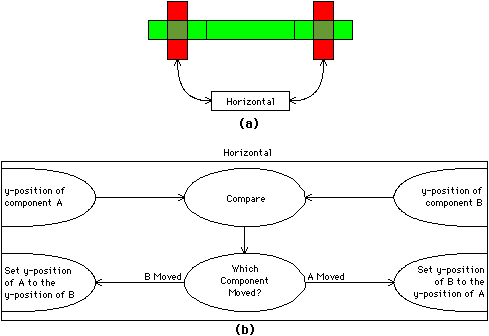 |
| FIGURE 1.28 Graphical layout constraint: (a) Layout (b) Constraint contents. |
|
Previous |  |
Table of Contents | Next | |
Static Free Software |  |