 |
 |
|
|
Layout-level environments exist primarily for the generation of final manufacturing specifications. Every component in these environments has precise dimensions, and its location in the design corresponds exactly to its final position in the manufactured circuit. Although some layout-level environments have information about higher levels of design, this information is not mandatory. For example, nMOS design can include connectivity information, behavioral descriptions, and links to equivalent circuits in other environments. Ultimately, however, all that matters is the geometry of the layout, so it is acceptable for the nMOS environment to contain only rectangles as primitives. The needs of the designer determine the complexity of these layout environments.
Three different types of layout environments are worth mentioning here. First, the integrated-circuit domain includes the MOS, bipolar, gallium arsenide, and other microsilicon environments. MOS devices have received much attention lately as a desirable medium in which to build large systems [Glasser and Dobberpuhl]. Second, the macro electronic environments include printed-circuit-board design, wire-wrap-board design, and others of that ilk. These environments have been used to build large systems for many years. Finally, the pure artwork environment exists for the generation of graphics, not electronics, and is useful in its own right as well as in combination with circuit layout.
Besides providing different layout environments, a good design system should allow these components to be intermixed. Mixed environment designs are useful for process experimentation, in which new structures are being combined. They are also valuable in design when partial layout is used with schematics or other nonspecific components. Finally, mixed environments are useful in large system designs that demand interconnection of many components that are not of uniform origin.
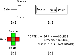
The n-channel metal oxide semiconductor environment is one of two MOS environments that will be discussed. The distinguishing characteristic of MOS is its use of a field-effect transistor to do switching. In this type of transistor, the switching element runs over the switched line, causing a field to be produced at the intersection (see Fig. 1.18b). This field conditionally inhibits the flow of current in the switched line. An algorithm that has been reduced to a collection of logic gates can be implemented in the MOS environments. This is because all logical operations can be implemented with combinations of these transistors.
There are different layers of conducting and semiconducting material that are available for the implementation of nMOS. The switching layer is polysilicon and is colored red in this book. The switched layer is diffusion and is colored green. These two layers cannot cross each other without forming a component: either a transistor or a direct contact. To make general-purpose connections that do not interfere with other layers, there is a metal layer, colored blue, which can cross polysilicon or diffusion without connecting. Special contacts can be used, however, to connect metal to the other layers.
These three layers are the only ways to run wires in an nMOS circuit, although some fabrication processes have an extra layer of metal or polysilicon. There are, however, many other layers that are used to make a chip. An implant region, colored yellow, is used over the switching area of a transistor to set it permanently "on." This alternate kind of transistor is useful for obtaining the appropriate voltage levels needed to implement logical functions. The direct connections between metal, polysilicon, and diffusion use intermediate layers such as the contact-cut and the buried-contact layers. The entire chip is typically covered with a layer of protective coating called overglass, which must be removed at the bonding pads to allow the chip to be externally wired. And to make things even more complicated, some nMOS fabrication processes have special layers, such as light implant, hard or light enhancement, and secondary contact, which are rarely, if ever, used during layout.
Given that there are many layers and that geometry is the only important result, one is tempted to provide a purely geometric set of design components for the nMOS environment. In fact, any implementation of the nMOS environment that does not have components for specifying arbitrary shapes on all the layers is likely to fall short of the designer's needs. However, it is possible to provide more complex components that will make much of the design phase easier. If these components form a consistent view of nMOS at some higher level of design, then the problems of conversion in and out of this environment will be lessened. Also, layout environments will be able to cater to circuit designers if these components include connectivity.
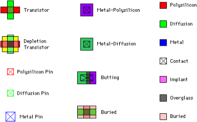 |
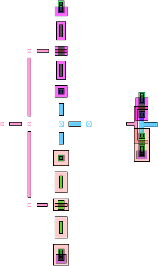
| FIGURE 2.18 The primitive components of the nMOS environment. Transistors and intralayer pins are on the left; interlayer contacts are in the center; basic-layer components are on the right. |
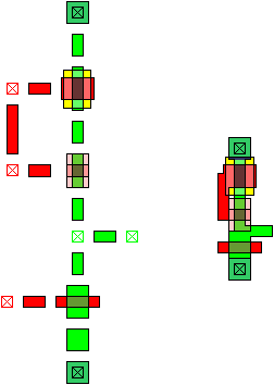
| Figure 2.18 shows a set of high-level primitives that can be used for nMOS design. These components, used by the Electric system (see Chapter 11), have been adequate for the layout of medium- to large-scale ICs. There are, of course, the two types of transistors in this environment: enhancement (the normal polysilicon over diffusion) and depletion (with the implant layer). In addition, there are four basic layer-to-layer contacts: a metal-to-polysilicon, a metal-to-diffusion, a triple-layer butting contact, and a polysilicon-to-diffusion buried contact. In order to connect these components, there are wires that can run in all three layers. These wires can make junctions to themselves with the three pin components. Finally, the right side contains basic-layer components that can be used to make any geometric structure. The design of an inverter with these primitives is illustrated in Fig. 2.19. |
|
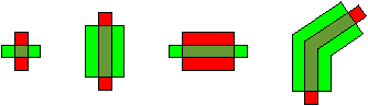
| In order to encourage their use, these nMOS primitives must be more flexible than they appear in Fig. 2.18. For example, the transistor component should be able to scale properly in either dimension and even to bend (see Fig. 2.20). Also, the contacts should be available in other configurations, either by having extra primitive components or by parameterizing the components that are there. |
|
The use of advanced design components in a layout-level environment such as nMOS does not hinder the flexibility of circuits that can be built. Circuit and VLSI designers prefer to deal with such a set of primitives because it agrees with their connectivity-oriented view of circuitry. For mask designers, the transistor and contact primitives can be ignored so that design can be done solely with geometric components. However, many mask designers understand enough about circuitry to appreciate these higher-level primitives. In fact, some designers prefer to use cell libraries with even-higher-level primitives that perform complex circuit functions [Newkirk and Mathews]. All that is needed for any designer is a small but powerful set of components that produces correct layout while providing information relevant to the task at hand.
The complementary metal oxide semiconductor (CMOS) environment is very similar to the n-channel MOS devices previously discussed. As in all MOS environments, a field-effect transistor is used that is simple enough to be modeled with a few components. Also, as in all MOS environments, there is a polysilicon layer that gates a diffusion layer, and one or more metal layers that can run anywhere. There are also contact structures, special implant layers, optional additional polysilicon layers, and an overglass layer for chip protection. In other respects, however, CMOS and nMOS are quite dissimilar.
CMOS design is a wholly different way of thinking about circuits [Weste and Eshraghian]. In nMOS, the enhancement transistor is a gate and the depletion transistor is used to obtain a "weak" logical high or becomes logically low by being gated to ground. Thus nMOS design centers around the operations that make a signal either weakly high or strongly low. This asymmetry means that certain transitions take longer to complete (setting a signal high takes longer than setting it low) and that certain states take much more power (holding a signal low consumes more power). The amount of space used in an nMOS design is small, but the power and speed characteristics are limiting.
In CMOS there are two transistors that either open the gate when on, or open the gate when off. There are no weak truth values and so the speed of any operation is as fast as the fastest nMOS action. Power requirements are also lower. The only problem is that every operation must be duplicated and this uses larger amounts of space. Fortunately, the space costs are not always of major concern and there are dynamic design styles that reduce the area [Weste and Eshraghian]. For all these reasons, CMOS is rapidly becoming the most popular integrated-circuit environment.
Because the two CMOS transistors perform logically opposite functions, they and all of their connecting diffusion wires must be enveloped in implant areas that dictate the sense of the function. The CMOS designer must therefore consider not only metal, polysilicon, and diffusion, but also implant regions: well and/or native substrate.
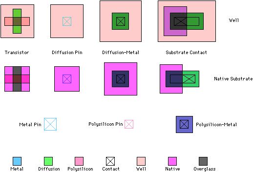 |
| FIGURE 2.21 The components of the CMOS environment. Top two rows are implant-sensitive components. Bottom row contains basic-layer components. |
| Designing an environment for CMOS can take many paths. In addition to having a set of geometric primitives for the mask designer, the environment can provide contacts and transistors for use by chip designers. Given that all diffusion paths are implant sensitive, however, these higher-level transistor and contact primitives will fall short of completing the layout, because the implant areas will have to be specified with lower-level primitives. The solution, shown in Fig. 2.21, is to define two sets of diffusion-related primitives for the two implant regions. This means that, in addition to having two transistors, there are two types of diffusion wire, two wire junction pins for diffusion, and two metal-to-diffusion contacts. This allows the design to be done without undue considerations for the implant regions, because most of these layers will appear as a byproduct of using the proper components and wires. Figure 2.22 shows a CMOS inverter made from these components. |
|
CMOS illustrates the problem of having too many layers to manipulate conveniently. In typical environments, the design is so confusing that a set of standard cells is made and used for all layout, thus avoiding the need to deal with the complexities of this environment [Feller]. Standard-cell packages change the nature of the design environment by providing high-level primitives. In addition, they can impose their own design methodologies that totally redefine the nature of the layout task [Schediwy]. However, direct CMOS layout can still be accomplished by simplifying the design components to a manageable and consistent set, so that confusion is reduced and design is more easily done.
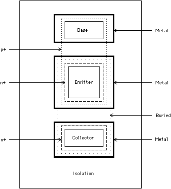
| The bipolar environments form a family, much like the MOS family. Many notions can be shared among the members of this family, and many aspects are different. One commonality is that the basic switch for the bipolar environments is a junction transistor, which has a base, an emitter, and a collector. This transistor is much different in structure from, and is more complex than, the field-effect transistor used in MOS (see Fig. 2.23). Also, bipolar environments rarely make component connections with semiconducting material: Usually metal wires are the only ones used. |
|
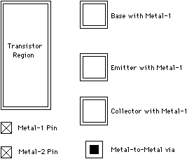
| A sample bipolar environment is shown in Fig. 2.24. The transistor is an empty implant region into which base, emitter, and collector components can be placed. These components have metal surrounding them because metal is the only way to make a connection. However, the many other layers needed to specify a bipolar circuit precisely are not shown, because they can be automatically derived from these simpler components [Szabo, Leask and Elmasry]. The bipolar environment shown here has two layers of metal, so it needs two metal pins and an intermetal contact (called a via). Some bipolar environments also have polysilicon or a third metal layer. |
|
The flexibility of designing custom transistors, resistors, and diodes is exactly what is needed in a bipolar environment. The limited set of transistors available in MOS is not sufficient. Instead, the transistor must be broken down into its basic components in order to satisfy the designer. Note, however, that some sensible combinations of layers can be made as in the case of the bases, emitters, collectors, and the via. By insisting that the components of a transistor all connect to the transistor implant area, the design system can still treat transistors as single objects and capture more information for the circuit designer. Thus even in a very low-level environment such as this, it is possible to provide more than purely geometric design primitives.
Integrated-circuit (IC) packages are the component-level environment of choice today. Most algorithm design is converted to this for implementation, because this is the medium that is commonly available. Standardized voltage levels allow these packages to be directly interconnected and standard pin spacings allow them to be physically connected.
| A typical IC package has two rows of wires running on either side of a plastic or ceramic body (see Fig. 2.25). These chips, called dual inline packages (DIPs) always have the wire leads spaced 0.1 inch apart or multiples thereof. DIPs can have as few as two pins but typically have 14 or 16 pins and occasionally have over 100. Some packages have a single row of pins and are single inline packages. Recently, packages have appeared with pins on all four sides, called quad packages. In addition, there are packages with pins spaced uniformly across the underside, and they are called pin grid arrays. |
|
Package connections depend on the surface to which the packages are attached. A wire-wrap board is one that has pin sockets on one side attached to long terminal posts on the other. The ICs plug into the side of the board with sockets and the wires run between the terminals on the other side.
Printed-circuit boards are a less flexible method of connecting IC packages because they are more permanent. The packages are soldered to the board and the wiring is etched along the board surface, making all changes difficult. Because they are more permanent, printed-circuit boards are used in production designs that need no debugging, but do need to be produced inexpensively. Many printed-circuit boards contain multiple layers of wire paths. This allows complex connectivity without the problems of path crossing. Simple multilayer boards have wiring on two sides but some printed-circuit boards have six or more layers.
The integrated-circuit packages have a wide range of complexity. Early packages were called SSI, or small-scale integration. This meant that a handful of gate-level components could be built into a single package. For example, the contents of the package in Fig. 2.25 is of SSI complexity. The power and ground pins must be connected to standard voltages (TTL designs use +5v and 0v respectively) and the levels on the logic gate pins also use standard voltages (higher than a threshold for true, lower for false). This particular SSI package has four NAND gates, each with two inputs. Typically, anything with up to 40 logic gates is within the realm of SSI.
More advanced packages are in the MSI family (medium-scale integration). The logic diagram in Fig. 1.11 is typical of the complexity of MSI packages. In this family, the complexity limit is about 500 gates, although this number and all other family distinctions are somewhat arbitrary.
Even more complex integrated circuits are LSI, or large-scale integration. The capabilities of a single LSI chip include memories (one million bits in a package), multipliers (16-bit parallel multiplication), and processors (Z80 or MC68000 single-chip processors). LSI chips can be as complex as one million gates.
Beyond LSI is VLSI (very-large-scale integration) and the promise of ULSI (ultra-large-scale integration). Such chips have so much information that the management of their design presents difficulty for some design systems. Currently, complex systems are being built in WSI (wafer-scale integration), in which hundreds of integrated circuits interconnect on a single wafer. Entire architecture-level descriptions can be embodied in a single VLSI system, causing a paradox in the notion that integrated-circuit packages are at the component level of design. This only confirms the futility of trying to categorize environments: What is an entire architecture to one designer is merely a component in a layout to someone else.
Artwork is not electrical. An artwork environment is simply a set of components for the design of arbitrary graphics. These graphics can be used to embellish circuit layouts (which is common in PC-board and chip layout) or they can be used independently of electronics; for example, to make figures for papers and slides. In any case, an artwork environment must be able to do any kind of layout, so a first reaction is to make this environment have a few basic geometric components such as a line, a polygon, a circle, and some text.
A look at any sketchpad editor, however, will reveal that complex primitives are often provided to the artist. Arrowheads, triangles, splines, and many more shapes appear in design menus. Even circuit and other scientific symbols can be found. Thus the existence of this environment in conjunction with the other electronic environments described here can be beneficial, given that components from all environments can be mixed in a single design. Since a CAD system must provide the graphical human interface, I/O, database facilities, and design primitives, it may as well throw in a few purely graphical components and be truly useful.
|
Previous |  |
Table of Contents | Next | |
Static Free Software |  |