 |
 |
|
|
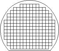
Integrated circuits are manufactured on large disks of silicon called wafers. A group of about 20 of these wafers is called a boatload and a large collection of boatloads manufactured together is called a run or a batch. A wafer is round, from 3 to 6 inches in diameter, and has one side flattened (see Fig. 4.21). Although it can contain hundreds of different IC dies, there is typically only one type of chip on a wafer and it is replicated in all but a few of the die locations. Some prototyping operations combine multiple chip dies on a single wafer, or place multiple IC designs into a single die. Also, there are occasional test dies inserted at various locations on the wafer. The placement of a different die on an otherwise uniform mask is called a drop-in. The entire production process is illustrated in Fig. 7.3.
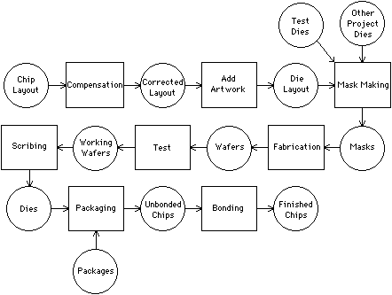 |
| FIGURE 7.3 Chip manufacturing steps. |
A wafer consists of multiple layers of conducting and semiconducting material. Each layer is specified with a mask that controls the deposition or etching of material during fabrication. Masks are produced either optically or by electron-beam techniques, and always under computer control. In some prototyping situations, the mask is not used and an electron-beam device writes directly on the wafer. Regardless of the masking technology, the controlling formats are the same.
Although there are many mask-manufacturing formats and interchange formats targeted at mask making, there are a few standards that will be discussed here. Caltech Intermediate Format (CIF) and Calma GDS II Stream Format are well-known interchange standards, whereas Electronic Design Interchange Format (EDIF) is newer and less popular, but its vast extent may carry it to a wide acceptance. The Electron Beam Exposure System (EBES) format is an actual machine specification, like the Gerber format.
Caltech Intermediate Format (CIF) is a simple method for describing integrated circuits [Hon and Sequin]. The goals of CIF are to be concise, to be readable by humans and machines, and most of all to remain constant so that it can be relied on as a standard. Its authors have allowed "user extensions," but permit no change to the basic commands. Appendix B describes CIF in detail.
A CIF file is a set of textual commands to set layers and draw on them. CIF describes only the geometry that is found on IC masks: rectangles, polygons, wires, and circular pads. There are no higher-level graphics operations such as text or curves. There is hierarchy, however, which makes CIF easy to generate and can be used to build complex graphics. In addition, the language is structured to allow multiple CIF files to easily be aggregated into a single larger file so that multiproject chips can be specified. The only drawback of CIF is that it is not readable by any mask-making machines and thus must be further processed before it can be used in fabrication.
Calma GDS II Stream Format is older than CIF and is more widely used [Calma]. Its early entry in the market caused subsequent vendors to accept it for compatibility reasons; thus it became a standard. In addition to representing mask geometry, it also has facilities for topological information and arbitrary other attributes. The reason for this is that GDS II is the complete database representation for Calma CAD systems, and not just the output specification for mask-making. Thus it includes text, arrays, structures, and hierarchy (see Appendix C).
GDS II has changed over the years as new constructs have been introduced. Nevertheless, backward compatibility has been maintained, which has allowed the format to remain the industry standard. Like CIF, this is an intermediate format that must be converted before it can be made into a mask. The other drawback of GDS II is that it is binary, which makes it not readable by humans. Some would argue that these formats are not meant for humans and that binary provides more compaction of data. However, the CAD programmer does appreciate a readable format and, as far as compaction is concerned, a concise text language such as CIF does not use much more space.
The most recent VLSI interchange format is the Electronic Design Interchange Format (EDIF), which was proposed by a consortium of electronics companies [EDIF Committee]. There is hope that this format will replace others as the standard, because it is so powerful, easy to parse, and still open to the future needs of CAD systems. Additionally, many CAD vendors have promised EDIF compatibility in their products [VLSI Design]. The format is described in Appendix D.
EDIF is a textual format that resembles the LISP programming language [McCarthy et al.]. Each statement is enclosed in parentheses and has a keyword first, followed by its parameters. Also, the entire EDIF file is structured so that all statements are parameters to other statements. This means that an EDIF file has only one statement:
(edif ediffile)
(library name libcontents)
(cell name cellcontents)
Although EDIF ambitiously attempts to include everything of interest to a
CAD system, the specification is imperfect in a number of areas, as even
the EDIF committee acknowledges.
Behavior and constraints are poorly understood, so the specification
merely mentions the need for this information without suggesting how
it can be done.
Also, there is a definite problem with wordiness and overspecification.
Some of the ordering of the syntax is set so that identifiers are used
before they are first declared (for example, the viewmap section,
which associates different views of a cell, must come before the views).
This makes parsing more difficult.
Even the so-called human readability of EDIF could be improved if
some of the long keywords such as portimplementation had dashes or
hyphens to help separate the individual words that compose them.
A cleaner and more complete scheme for this kind of information is SHIFT [Liblong], which was proposed earlier but was not selected as a standard. This interchange format has well-specified behavior and constraints as well as the capability of describing topology and geometry. It is remarkable that SHIFT is so similar to EDIF in structure and intent. It even has LISPlike syntax.
EDIF does provide nonstandard escape mechanisms so that additional information can be included. This could be useful, for example, when specifying non-Manhattan orientations of cell instances that are not yet supported in EDIF. Since the standard openly admits that it is incomplete, these extensions will soon be accepted. However, care must be exercised by the CAD system designer to ensure that these extensions are properly coordinated and well thought out, or else EDIF will diverge and fail to be a standard.
Sooner or later the CAD system must produce a chip description that can be read by a mask-making machine. With today's smaller IC features, it is becoming clear that the electron-beam lithography methods are preferable to optical techniques. Within the domain of electron-beam devices, a very popular format is EBES, the Electron Beam Exposure System developed at Bell Laboratories [Gross, Raamot, and Watkins].
EBES is readable directly by a number of different mask-making machines and this explains why it allows no hierarchy. Although these machines have computers in them, they spend all their time driving the electron beam and cannot accept a complex input format. In fact, there are only three different figures that can be drawn: rectangles, parallelograms, and trapezoids. Everything else must be composed from these. Although some machines have allowed extensions to EBES such as arrays and extended addressing, the original format is the only guaranteed standard.
The major drawback of EBES format is that it is binary and that the binary word size is restrictively small for modern tasks. With only 16-bit words, a complete chip must be described in a square of only 65,536 units on a side. This used to be a large field but it is easily exceeded today, forcing chips to be described as multiple abutting dies. Another problem with EBES, as Appendix E shows, is that the geometry must be sorted so that it is presented to the electron-beam machine in spatial order. This geometry must be clipped into stripes and then all the pieces must be sorted by y coordinate. Rounded figures must be approximated by polygons and complex polygons must be broken into four-sided figures. Combined with a lack of hierarchy, these problems cause EBES files to be large and slow to produce.
In this discussion of IC manufacturing specification, it is appropriate to discuss the final steps: packaging and bonding. Packaging is the selection and attachment of the IC die to a plastic or ceramic chip body that has metal leads [Johnson and Lipman]. Bonding is the step that runs wires from the chip body's leads to the IC pads on the die. Both of these steps belong in a CAD system although they are more commonly done by hand.
Packaging options for ICs change very often so it would be helpful if the CAD system maintained a database of packages showing the number of pins, the external pin arrangement, the internal cavity size for the die, and other physical package properties. The system could then help to select the most appropriate package for the task at hand.
Programmable bonding machines do exist to wire integrated-circuit pads to the chip package leads. However, they typically work in an interactive-learning mode that requires an operator to bond one chip completely before the machine can do more. Subsequent chips are then automatically inspected to locate special fiducial marks so that variances in orientation can be handled. It would certainly be reasonable to link the CAD system with this machine so that it knows the placement of all of the pads and needs no human instruction.
|
Previous |  |
Table of Contents | Next | |
Static Free Software |  |