Copyright Michael Karbo and ELI Aps., Denmark, Europe.
Chapter 9. Moores' Law
This development was actually described many years ago, in what we call Moores Law.
|
Right back in 1965, Gordon Moore predicted (in the Electronics journal), that the number of transistors in processors (and hence their speed) would be able to be doubled every 18 months. |
|

If we try to look ahead in time, we can work out that in 2010 we should have processors containing 3 billion transistors. And with what clock frequencies? Youll have to guess that for yourself.
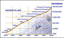 Fig. 59.
 Process technology
The many millions of transistors inside the CPU are made of, and connected by, ultra thin electronic tracks. By making these electronic tracks even narrower, even more transistors can be squeezed into a small slice of silicon.
The width of these electronic tracks is measured in microns (or micrometers), which are millionths of a metre.
For each new CPU generation, the track width is reduced, based on new technologies which the chip manufacturers keep developing. At the time of writing, CPUs are being produced with a track width of 0.13 microns, and this will be reduced to 0.09 and 0.06 microns in the next generations.
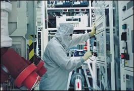 Fig. 60. CPUs are produced in extremely
high-technology environments (clean rooms). Photo courtesy of AMD.
Fig. 60. CPUs are produced in extremely
high-technology environments (clean rooms). Photo courtesy of AMD.
In earlier generations aluminium was used for the current carrying tracks in the chips. With the change to 0.18 and 0.13-micron technology, aluminium began to be replaced with copper. Copper is cheaper, and it carries current better than aluminium. It had previously been impossible to insulate the copper tracks from the surrounding silicon, but IBM solved this problem in the late 1990s.
AMD became
the first manufacturer to mass-produce CPUs with copper tracks in their chip
factory fab
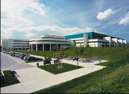 Fig. 61. AMDs Fab
 A grand new world
We can expect a number of new CPUs in this decade, all produced in the same way as they are now just with smaller track widths. But there is no doubt that we are nearing the physical limits for how small the transistors produced using the existing technology can be. So intense research is underway to find new materials, and it appears that nanotransistors, produced using organic (carbon-based) semiconductors, could take over the baton from the existing process technology.
Bell Labs
in the
Less power consumption
The types of CPUs we have today use a fairly large amount of electricity when the PC is turned on and is processing data. The processor, as you know, is installed in the motherboard, from which it receives power. There are actually two different voltage levels, which are both supplied by the motherboard:
As the track width is reduced, more transistors can be placed within the same area, and hence the voltage can be reduced.
As a consequence of the narrower process technology, the kernel voltage has been reduced from 3 volts to about 1 volt in recent years. This leads to lower power consumption per transistor. But since the number of transistors increases by a corresponding amount in each new CPU generation, the end result is often that the total power consumption is unchanged.
 Fig. 62. A powerful fan. Modern CPUs require
something like this.
Fig. 62. A powerful fan. Modern CPUs require
something like this.
It is very important to cool the processor; a CPU can easily burn 50-120 Watts. This produces a fair amount of heat in a very small area, so without the right cooling fan and motherboard design, a Gigahertz processor could quickly burn out.
Modern processors contain a thermal diode which can raise the alarm if the CPU gets to hot. If the motherboard and BIOS are designed to pay attention to the diodes signal, the processor can be shut down temporarily so that it can cool down.
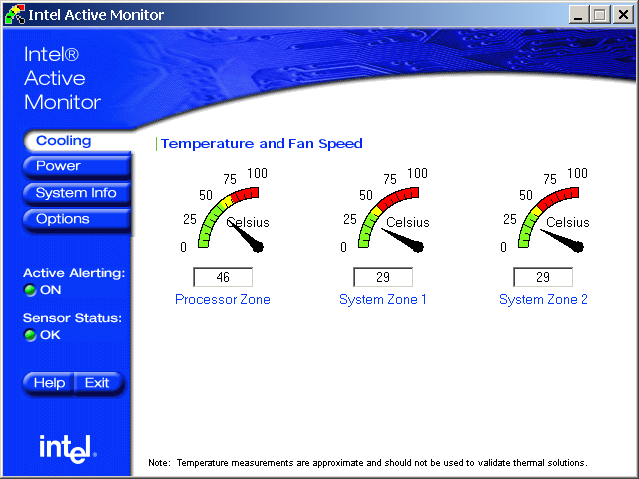 Figur 63. The temperatures on the
motherboard are constantly reported to this program..
Figur 63. The temperatures on the
motherboard are constantly reported to this program..
Cooling is a whole science in itself. Many nerds try to push CPUs to work at higher clock speeds than they are designed for. This is often possible, but it requires very good cooling and hence often huge cooling units.
30 years development
Higher processor speeds require more transistors and narrower electronic tracks in the silicon chip. In the overview in Fig. 64 you can see the course of developments in this area.
Note that the 4004 processor was never used for PCs. The 4004 was Intels first commercial product in 1971, and it laid the foundation for all their later CPUs. It was a 4-bit processor which worked at 108 KHz (0.1 MHz), and contained 2,250 transistors. It was used in the first pocket calculators, which I can personally remember from around 1973-74 when I was at high school. No-one could have predicted that the device which replaced the slide rule, could develop, in just 30 years, into a Pentium 4 based super PC.
If, for
example, the development in automobile technology had been just as fast, we
would today be able to drive from
|
Year |
Intel CPU |
Technology (track width) |
|
1971 |
4004 |
10 microns |
|
1979 |
8088 |
3 microns |
|
1982 |
80286 |
1.5 microns |
|
1985 |
80386 |
1 micron |
|
1989 |
80486 |
1.0/0.8 microns |
|
1993 |
Pentium |
0.8/0.5/0.35 microns |
|
1997 |
Pentium II |
0.28/0.25 microns |
|
1999 |
Pentium III |
0.25/0.18/0.13 microns |
|
2000-2003 |
Pentium 4 |
0.18/0.13 microns |
|
2004-2005 |
Pentium
4 |
0.09 microns |
Fig. 64. The high clock frequencies are the result of new process technology with smaller electronic tracks.
A conductor which is 0.09 microns (or 90 nanometres) thick, is 1150 times thinner than a normal human hair. These are tiny things we are talking about here.
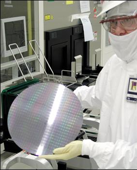
Wafers and die size
Another CPU measurement is its die size. This is the size of the actual silicon sheet containing all the transistors (the tiny area in the middle of Fig. 33 on page 15).
At the chip factories, the CPU cores are produced in so-called wafers. These are round silicon sheets which typically contain 150-200 processor cores (dies).
The smaller one can make each die, the more economical production can become. A big die is also normally associated with greater power consumption and hence also requires cooling with a powerful fan (e.g. see Fig. 63 on page 25 and Fig. 124 on page 50).
You can see the measurements for a number of CPUs below. Note the difference, for example, between a Pentium and a Pentium II. The latter is much smaller, and yet still contains nearly 2½ times as many transistors. Every reduction in die size is welcome, since the smaller this is, the more processors can fit on a wafer. And that makes production cheaper.
|
CPU |
Track width |
Die size |
Number of |
|
Pentium |
0.80 |
294 mm2 |
3.1 mil. |
|
Pentium MMX |
0.28 |
140 mm2 |
4.5 mil. |
|
Pentium II |
0.25 |
131 mm2 |
7.5 mil. |
|
Athlon |
0.25 |
184 mm2 |
22 mil. |
|
Pentium III |
0.18 |
106 mm2 |
28 mil. |
|
Pentium III |
0.13 |
80 mm2 |
28 mil. |
|
Athlon XP |
0.18 |
128 mm2 |
38 mil. |
|
Pentium 4 |
0.18 |
217 mm2 |
42 mil. |
|
Pentium 4 |
0.13 |
145 mm2 |
55 mil. |
|
Athlon XP+ |
0.13 |
115 mm2 |
54 mil. |
|
Athlon 64 FX |
0,13 |
193 mm2 |
106 mill. |
|
Pentium 4 |
0.09 |
112 mm2 |
125 mil. |
Fig. 66. The smaller the area of each processor core, the more economical chip production can be.
The modern CPU generations
As mentioned earlier, the various CPUs are divided into generations (see also Fig. 56 on page 23).
At the time of writing, we have started on the seventh generation. Below you can see the latest processors from Intel and AMD, divided into these generations. The transitions can be a bit hazy. For example, Im not sure whether AMDs K6 belongs to the 5th or the 6th generation. But as a whole, the picture is as follows:
|
Generation |
CPUs |
|
5th |
Pentium, Pentium MMX, K5, K6 |
|
6th |
Pentium Pro, K6-II, Pentium II, K6-3, Athlon, Pentium III |
|
7th |
Pentium 4, Athlon XP |
|
8th. |
Athlon 64 FX, Pentium 5 |
Fig. 67. The latest generations of CPUs.