Copyright Michael Karbo and ELI Aps., Denmark, Europe.
Chapter 12. Data and instructions
Now its time to look more closely at the work of the CPU. After all, what does it actually do?
Instructions and data
Our CPU processes instructions and data. It receives orders from the software. The CPU is fed a gentle stream of binary data via the RAM.
These instructions can also be called program code. They include the commands which you constantly via user programs send to your PC using your keyboard and mouse. Commands to print, save, open, etc.
Data is typically user data. Think about that email you are writing. The actual contents (the text, the letters) is user data. But when you and your software say send, your are sending program code (instructions) to the processor:
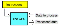 Fig. 80. The instructions process the user
data.
Fig. 80. The instructions process the user
data.
Instructions and compatibility
Instructions are binary code which the CPU can understand. Binary code (machine code) is the mechanism by which PC programs communicate with the processor.
All processors, whether they are in PCs or other types of computers, work with a particular instruction set. These instructions are the language that the CPU understands, and thus all programs have to communicate using these instructions. Here is a simplified example of some machine code instructions written in the language the processor understands:
proc near
mov AX,01
mov BX,01
inc AX
add BX,AX
You can no doubt see that it wouldnt be much fun to have to use these kinds of instructions in order to write a program. That is why people use programming tools. Programs are written in a programming language (like Visual Basic or C++). But these program lines have to be translated into machine code, they have to be compiled, before they can run on a PC. The compiled program file contains instructions which can be understood by the particular processor (or processor family) the program has been coded for:
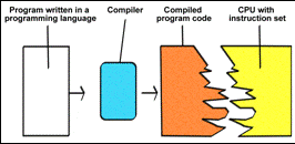 Fig. 81. The program code produced has to
match the CPUs instruction set. Otherwise it cannot be run.
Fig. 81. The program code produced has to
match the CPUs instruction set. Otherwise it cannot be run.
The processors from AMD and Intel which we have been focusing on in this guide, are compatible, in that they understand the same instructions.
There can be big differences in the way two processors, such as the Pentium and Pentium 4, process the instructions internally. But externally from the programmers perspective they all basically function the same way. All the processors in the PC family (regardless of manufacturer) can execute the same instructions and hence the same programs.
And thats precisely the advantage of the PC: Regardless of which PC you have, it can run the Windows programs you want to use.
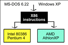
As the years have passed, changes have been made in the instruction set along the way. A PC with a Pentium 4 processor from 2002 can handle very different applications to those which an IBM XT with an 8088 processor from 1985 can. But on the other hand, you can expect all the programs which could run on the 8088, to still run on a Pentium 4 and on a Athlon 64. The software is backwards compatible.
The entire software industry built up around the PC is based on the common x86 instruction, which goes back to the earliest PCs. Extensions have been made, but the original instruction set from 1979 is still being used.
x86 and CISC
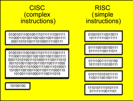
People sometimes differentiate between RISC and CISC based CPUs. The (x86) instruction set of the original Intel 8086 processor is of the CISC type, which stands for Complex Instruction Set Computer.
That means that the instructions are quite diverse and complex. The individual instructions vary in length from 8 to 120 bits. It is designed for the 8086 processor, with just 29,000 transistors. The opposite of CISC, is RISC instructions.
RISC stands for Reduced Instruction Set Computer, which is fundamentally a completely different type of instruction set to CISC. RISC instructions can all have the same length (e.g. 32 bits). They can therefore be executed much faster than CISC instructions. Modern CPUs like the AthlonXP and Pentium 4 are based on a mixture of RISC and CISC.
In order to maintain compatibility with the older DOS/Windows programs, the later CPUs still understand CISC instructions. They are just converted to shorter, more RISC-like, sub-operations (called micro-ops), before being executed. Most CISC instructions can be converted into 2-3 micro-ops.
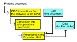 Fig. 84. The CISC instructions are decoded
before being executed in a modern processor. This preserves compatibility with
older software.
Fig. 84. The CISC instructions are decoded
before being executed in a modern processor. This preserves compatibility with
older software.
Extensions to the instruction set
For each new generation of CPUs, the original instruction set has been extended. The 80386 processor added 26 new instructions, the 80486 added six, and the Pentium added eight new instructions.
At the same time, execution of the instructions was made more efficient. For example, it took an 80386 processor six clock ticks to add one number to a running summation. This task could be done in the 80486 (see page 40), in just two clock ticks, due to more efficient decoding of the instructions.
These changes have meant that certain programs require at least a 386 or a Pentium processor in order to run. This is true, for example, of all Windows programs. Since then, the MMX and SSE extensions have followed, which are completely new instruction sets which will be discussed later in the guide. They can make certain parts of program execution much more efficient.
Another innovation is the 64-bit extension, which both AMD and Intel use in their top-processors. Normally the pc operates in 32-bit mode, but one way to improve the performance is using a 64-bit mode. This requires new software, which is not available yet.
9. Inside the CPU
Instructions have to be decoded, and not least, executed, in the CPU. I wont go into details on this subject; it is much too complicated. But I will describe a few factors which relate to the execution of instructions. My description has been extremely simplified, but it is relevant to the understanding of the microprocessor. This chapter is probably the most complicated one in the guide you have been warned! Its about:
If we continue to focus on speeding up the processors work, this optimisation must also apply to the instructions the quicker we can shove them through the processor, the more work it can get done.
Pipelines
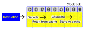
As mentioned before, instructions are sent from the software and are broken down into micro-ops (smaller sub-operations) in the CPU. This decomposition and execution takes place in a pipeline.
The pipeline is like a reverse assembly line. The CPUs instructions are broken apart (decoded) at the start of the pipeline. They are converted into small sub-operations (micro-ops), which can then be processed one at a time in the rest of the pipeline:
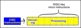 Fig. 85. First the CISC instructions are
decoded and converted into more digestible micro instructions. Then these are
processed. It all takes place in the pipeline.
Fig. 85. First the CISC instructions are
decoded and converted into more digestible micro instructions. Then these are
processed. It all takes place in the pipeline.
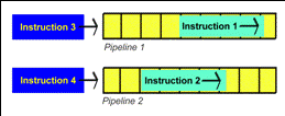
The pipeline is made up of a number stages. Older processors have only a few stages, while the newer ones have many (from 10 to 31). At each stage something is done with the instruction, and each stage requires one clock tick from the processor.
Modern CPUs have more than one pipeline, and can thus process several instructions at the same time. For example, the Pentium 4 and AthlonXP can decode about 2.5 instructions per clock tick.
The first Pentium 4 has several very long pipelines, allowing the processor to hold up to 126 instructions in total, which are all being processed at the same time, but at different stages of execution (see Fig. 88). It is thus possible to get the CPU to perform more work by letting several pipelines work in parallel:
CPU |
Instructions
executed |
|
AMD K6-II |
24 |
|
Intel Pentium III |
40 |
|
AMD Athlon |
72 |
|
Intel
Pentium 4 |
126 |
Fig. 88. By making use of more, and longer, pipelines, processors can execute more instructions at the same time.
The problems of having more pipelines
One might imagine that the engineers at Intel and AMD could just make even more parallel pipelines in the one CPU. Perhaps performance could be doubled? Unfortunately it is not that easy.
It is not possible to feed a large number of pipelines with data. The memory system is just not powerful enough. Even with the existing pipelines, a fairly large number of clock ticks are wasted. The processor core is simply not utilised efficiently enough, because data cannot be brought to it quickly enough.
Another problem of having several pipelines arises when the processor can decode several instructions in parallel each in its own pipeline. It is impossible to avoid the wrong instruction occasionally being read in (out of sequence). This is called misprediction and results in a number of wasted clock ticks, since another instruction has to be fetched and run through the assembly line.
Intel has tried to tackle this problem using a Branch Prediction Unit, which constantly attempts to guess the correct instruction sequence.
Length of the pipe
The number
of stations (stages) in the pipeline varies from processor to
processor. For example, in the Pentium II and III there are 10 stages, while
there are up to
In the Athlon, the ALU pipelines have 10 stages, while the FPU/MMX/SSE pipelines have 15.
The longer the pipeline, the higher the processors clock frequency can be. This is because in the longer pipelines, the instructions are cut into more (and hence smaller) sub-instructions which can be executed more quickly.
|
CPU |
Number of |
Maximum clock frequency |
|
Pentium |
5 |
300 MHz |
|
Motorola G4 |
4 |
500 MHz |
|
Motorola G4e |
7 |
1000 MHz |
|
Pentium II and III |
12 |
1400 MHz |
|
Athlon XP |
10/15 |
2500 MHz |
|
Athlon 64 |
12/17 |
>3000 MHz |
|
Pentium 4 |
20 |
>3000 MHz |
|
Pentium
4 |
31 |
>5000 MHz |
Fig. 89. Higher clock frequencies require long assembly lines (pipelines).
Note that the two AMD processors have different pipeline lengths for
integer and floating point instructions. One can also measure a processors efficiency
by looking at the IPC number (Instructions Per Clock), and AMDs Athlon
XP is well ahead of the Pentium
The same is even more true of the Motorola G4 processors used, for example, in Macintosh computers. The G4 only has a 4-stage pipeline, and can therefore, in principle, offer the same performance as a Pentium 4, with only half the clock frequency or less. The only problem is, the clock frequency cant be raised very much with such a short pipeline. Intel have therefore chosen to future-proof the Pentium 4 by using a very long pipeline.
Execution units
What is it that actually happens in the pipeline? This is where we find the so-called execution units. And we must distinguish between to types of unit:
If the processor has a brain, it is the ALU unit. It is the calculating device that does operations on whole numbers (integers). The computers work with ordinary text, for example, is looked after by the ALU.
The ALU is good at working with whole numbers. When it comes to decimal numbers and especially numbers with many decimal places (real numbers as they are called in mathematics), the ALU chokes, and can take a very long time to process the operations. That is why an FPU is used to relieve the load. An FPU is a number cruncher, specially designed for floating point operations.
There are typically several ALUs and FPUs in the same processor. The CPU also has other operation units, for example, the LSU (Load/Store Unit).
An example sequence
Look again at Fig. 73 on page 29. You can see that the processor core is right beside the L1 cache. Imagine that an instruction has to be processed:
This description applies to the working cycle in, for example, the Pentium III and Athlon. As a diagram it might look like this:
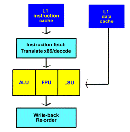 Fig. 90. The passage of instructions through the pipeline.
But the way the relationship between the pipeline and the execution units is designed differs greatly from processor to processor. So this entire examination should be taken as a general introduction and nothing more.
Pipelines in the Pentium 4
In the Pentium 4, the instruction cache has been placed between the Instruction fetch/Translate unit (in Fig. 90) and the ALU/FPU. Here the instruction cache (Execution Trace Cache) doesnt store the actual instructions, but rather the half-digested micro-ops.
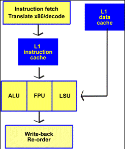 Fig. 91. In the Pentium 4, the instruction
cache stores decoded micro instructions.
Fig. 91. In the Pentium 4, the instruction
cache stores decoded micro instructions.
The actual pipeline in the Pentium 4 is longer than in other CPUs; it has 20 stages. The disadvantage of the long pipeline is that it takes more clock ticks to get an instruction through it. 20 stages require 20 clock ticks, and that reduces the CPUs efficiency. This was very clear when the Pentium 4 was released; all tests showed that it was much slower than other processors with the same clock frequency.
At the same time, the cost of reading the wrong instruction (misprediction) is much greater it takes a lot of clock ticks to fill up the long assembly line again.
The Pentium
4s architecture must therefore be seen from a longer-term perspective. Intel
expects to be able to scale up the design to work at clock frequencies of up to
5-10 GHz. In the
AMDs 32 bit Athlon line can barely make it much above a clock frequency of 2 GHz, because of the short pipeline. In comparison, the Pentium 4 is almost light years ahead.