Copyright Michael Karbo and ELI Aps., Denmark, Europe.
Chapter 14.Examples of CPUs
In this chapter I will briefly describe the important CPUs which have been on the market, starting from the PCs early childhood and up until today.
One could argue that the obsolete and discontinued models no longer have any practical significance. This is true to some extent; but the old processors form part of the family tree, and there are still legacies from their architectures in our modern CPUs, because the development has been evolutionary. Each new processor extended and built on top of an existing architecture.
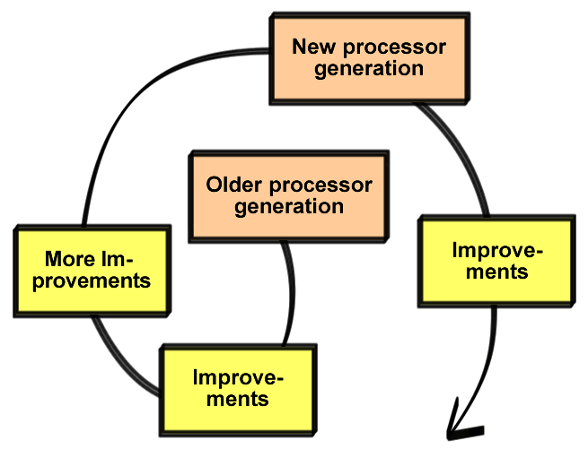 Fig. 98. The evolutionary development
spirals ever outwards.
Fig. 98. The evolutionary development
spirals ever outwards.
There is therefore value (one way or another) in knowing about the development from one generation of CPUs to the next. If nothing else, it may give us a feeling for what we can expect from the future.
16 bits the 8086, 8088 and 80286
The first PCs were 16-bit machines. This meant that they could basically only work with text. They were tied to DOS, and could normally only manage one program at a time.
But the original 8086 processor was still too good to be used in standard office PCs. The Intel 8088 discount model was therefore introduced, in which the bus between the CPU and RAM was halved in width (to 8 bits), making production of the motherboard much cheaper. 8088 machines typically had 256 KB, 512 KB or 1 MB of RAM. But that was adequate for the programs at the time.
The Intel 80286 (from 1984) was the first step towards faster and more powerful CPUs. The 286 was much more efficient; it simply performed much more work per clock tick than the 8086/8088 did. A new feature was also the 32 bit protected mode a new way of working which made the processor much more efficient than under real mode, which the 8086/8088 processor forced programs to work in:
Access to multitasking, which means that the operating system can run several programs at the same time.
Protected mode paved the way for the change from DOS to Windows, which only came in the 1990s.
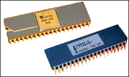 Fig. 99. Bottom: an Intel 8086, the first 16-bit processor. Top: the incredibly
popular 8-bit processor, the Zilog Z80, which the 8086 and its successors out
competed.
Fig. 99. Bottom: an Intel 8086, the first 16-bit processor. Top: the incredibly
popular 8-bit processor, the Zilog Z80, which the 8086 and its successors out
competed.
32 bits the 80386 and 486
The Intel 80386 was the first 32-bit CPU. The 386 has 32-bit long registers and a 32-bit data bus, both internally and externally. But for a traditional DOS based PC, it didnt bring about any great revolution. A good 286 ran nearly as fast as the first 386s under DOS anyway, since it doesnt exploit the 32-bit architecture.
The 80386SX became the most popular chip a discount edition of the 386DX. The SX had a 16-bit external data bus (as opposed to the DXs 32-bit bus), and that made it possible to build cheap PCs.
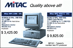 Fig. 100. Discount prices in October 1990 but only with a b/w monitor.
The fourth generation
The fourth generation of Intels CPUs was called the 80486. It featured a better implementation of the x86 instructions which executed faster, in a more RISC-like manner. The 486 was also the first CPU with built-in L1 cache. The result was that the 486 worked roughly twice as fast as its predecessor for the same clock frequency.
With the 80486 we gained a built-in FPU. Then Intel did a marketing trick of the type we would be better off without. In order to be able to market a cheap edition of the 486, they hit on the idea of disabling the FPU function in some of the chips. These were then sold under the name, 80486SX. It was ridiculous the processors had a built-in FPU; it had just been switched off in order to be able to segment the market.
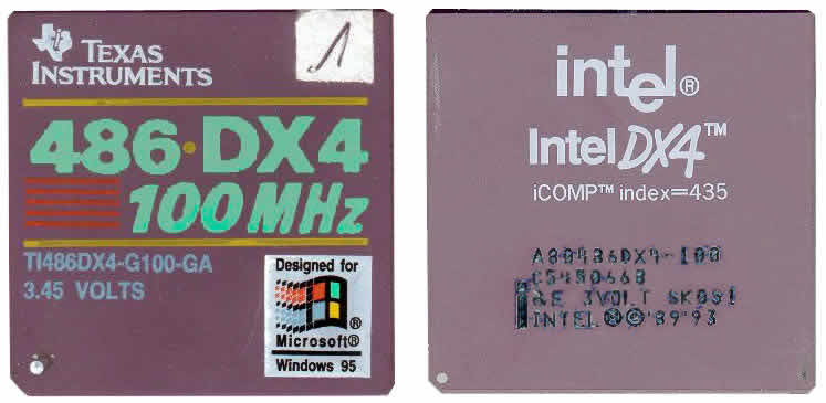 Fig. 101. Two 486s from two different
manufacturers.
Fig. 101. Two 486s from two different
manufacturers.
But the 486 was a good processor, and it had a long life under DOS, Windows 3.11 and Windows 95. New editions were released with higher clock frequencies, as they hit on the idea of doubling the internal clock frequency in relation to the external (see the discussion later in the guide). These double-clocked processors were given the name, 80486DX2.
A very popular model in this series had an external clock frequency of 33 MHz (in relation to RAM), while working at 66MHz internally. This principle (double-clocking) has been employed in one way or another in all later generations of CPUs. AMD, IBM, Texas Instruments and Cyrix also produced a number of 80486 compatible CPUs.
Pentium
In 1993 came the big change to a new architecture. Intels Pentium was the first fifth-generation CPU. As with the earlier jumps to the next generation, the first versions werent especially fast. This was particularly true of the very first Pentium 60 MHz, which ran on 5 volts. They got burning hot people said you could fry an egg on them. But the Pentium quickly benefited from new process technology, and by using clock doubling, the clock frequencies soon skyrocketed.
Basically, the major innovation was a superscalar architecture. This meant that the Pentium could process several instructions at the same time (using several pipelines). At the same time, the RAM bus width was increased from 32 to 64 bits.
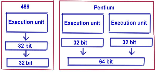 Fig. 102. The Pentium processor could be
viewed as two 80486s built into one chip.
Fig. 102. The Pentium processor could be
viewed as two 80486s built into one chip.
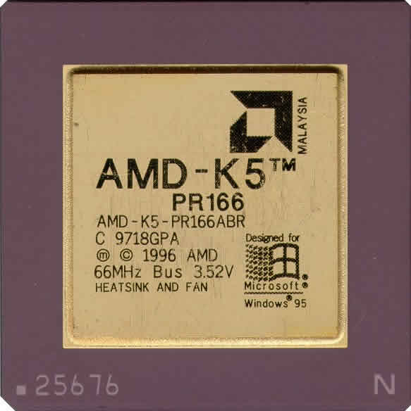
Throughout the 1990s, AMD gained attention with its K5 and K6 processors, which were basically cheap (and fairly poor) copies of the Pentium. It wasnt until the K6-2 (which included the very successful 3DNow! extensions), that AMD showed the signs of independence which have since led to excellent processors like the AthlonXP.
|
Fig. 103. One of the earlier AMD processors. Today youd hesitate to trust it to run a coffee machine |
In 1997, the Pentium MMX followed (with the model name P55), introducing the MMX instructions already mentioned. At the same time, the L1 cache was doubled and the clock frequency was raised.
Pentium II with new cache
After the Pentium came the Pentium II. But Intel had already launched the Pentium Pro in 1995, which was the first CPU in the 6th generation. The Pentium Pro was primarily used in servers, but its architecture was re-used in the popular Pentium II, Celeron and Pentium III models, during 1997-2001.
The Pentium II initially represented a technological step backwards. The Pentium Pro used an integrated L2 cache. That was very advanced at the time, but Intel chose to place the cache outside the actual Pentium II chip, to make production cheaper.
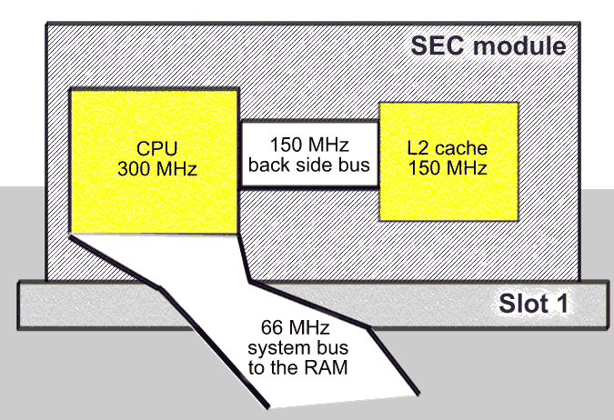 Fig. 105. L2 cache running at half CPU speed
in the Pentium II.
Fig. 105. L2 cache running at half CPU speed
in the Pentium II.
The Level 2 cache was placed beside the CPU on a circuit board, an SEC module (e.g. see Fig. 71, on page 28). The module was installed in a long Slot 1 socket on the motherboard. Fig. 106 shows the module with a cooling element attached. The CPU is sitting in the middle (under the fan). The L2 cache is in two chips, one on each side of the processor.
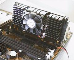 Fig. 106. Pentium II processor module mounted on its edge in the motherboards
Slot 1 socket (1997-1998).
Fig. 106. Pentium II processor module mounted on its edge in the motherboards
Slot 1 socket (1997-1998).
The disadvantage of this system was that the L2 cache became markedly slower than it would have been if it was integrated into the CPU. The L2 cache typically ran at half the CPUs clock frequency. AMD used the same system in their first Athlons. For these the socket was called, Slot A (see Fig. 107).
At some point, Intel decided to launch a discount edition of the Pentium II the Celeron processor. In the early versions, the L2 cache was simply scrapped from the module. That led to quite poor performance, but provided an opportunity for overclocking.
Overclocking means pushing a CPU to work at a higher frequency than it is designed to work at. It was a very popular sport, especially early on, and the results were good.
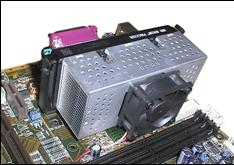 Fig. 107. One of the first AMD Athlon processors, mounted in a Slot A socket. See
the large cooling element.
Fig. 107. One of the first AMD Athlon processors, mounted in a Slot A socket. See
the large cooling element.
One of the problems of overclocking a Pentium II was that the cache chips couldnt keep up with the high speeds. Since these Celerons didnt have any L2 cache, they could be seriously overclocked (with the right cooling).
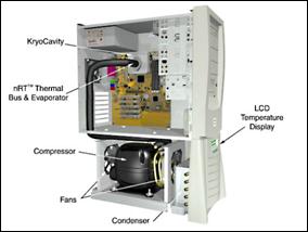 Fig. 108. Extreme CPU cooling using a
complete refrigerator built into the PC cabinet. With equipment like this,
CPUs can be pushed up to very high clock frequencies (See Kryotech.com and
Asetek.com).
Fig. 108. Extreme CPU cooling using a
complete refrigerator built into the PC cabinet. With equipment like this,
CPUs can be pushed up to very high clock frequencies (See Kryotech.com and
Asetek.com).
Intel later decided to integrate the L2 cache into the processor. That happened in a new versions of the Celeron in 1998 and a new versions of the Pentium III in 1999. The socket design was also changed so that the processors could be mounted directly on the motherboard, in a socket called socket 370. Similarly, AMD introduced their socket A.
Pentium 4 long in the pipe
The Pentium III was really just (yet) another edition of the Pentium II, which again was a new version of the Pentium Pro. All three processors built upon the same core architecture (Intel P6).
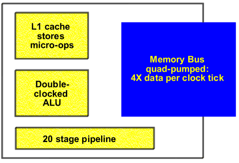
It wasnt until the Pentium 4 came along that we got a completely new processor from Intel. The core (P7) had a completely different design:
All of these factors are described elsewhere in the guide. The important thing to understand, is that the Pentium 4 represents a completely new processor architecture.