Copyright Michael Karbo and ELI Aps., Denmark, Europe.
Chapter 17. The CPUs immediate surroundings
In this part of this guide, we dug down into the inner workings of the CPU. We well let it rest in peace now, and concentrate on the processors immediate surroundings. That is, the RAM and the chipset or more precisely, the north bridge.In the first section of the guide I introduced the chipset, including the north bridge (see, for example, Fig. 46 on page 19), which connects the CPU to the PCs memory the RAM.
The pathway to RAM
The most important data path on the motherboard runs between the CPU and the RAM. Data is constantly pumped back and forth between the two, and this bus therefore often comes under focus when new generations of CPUs, chipsets and motherboards are released.
The RAM sends and receives data on a bus, and this work involves a clock frequency. This means that all RAM has a speed, just like a CPU does. Unfortunately RAM is much slower than the CPU, and the buses on the motherboard have to make allowance for this fact.
The XT architecture
In the original PC design (the IBM XT), the CPU, RAM and I/O devices (which we will come to later) were connected on one and the same bus, and everything ran synchronously (at a common speed). The CPU decided which clock frequency the other devices had to work at:
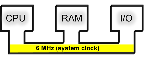
The problem with this system was that the three devices were locked to each other; they were forced to work at the lowest common clock frequency. It was a natural architecture in the first PCs, where the speed was very slow.
The first division of the bus
In 1987, Compaq hit on the idea of separating the system bus from the I/O bus, so that the two buses could work at different clock frequencies. By letting the CPU and RAM work on their own bus, independent of the I/O devices, their speeds could be increased.
In Fig. 119, the CPU and RAM are connected to a common bus, called the system bus, where in reality the CPUs clock frequency determines the working speed. Thus the RAM has the same speed as the CPU; for example, 12, 16 or 25 MHz.
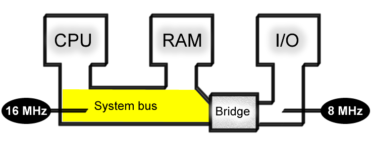 Fig. 119. With this architecture, the I/O bus is separate from the system bus
(80386).
Fig. 119. With this architecture, the I/O bus is separate from the system bus
(80386).
The I/O devices (graphics card, hard disk, etc.) were separated from the system bus and placed on a separate low speed bus. This was because they couldnt keep up with the clock frequencies of the new CPU versions.
The connection between the two buses is managed by a controller, which functions as a bridge between the two paths. This was the forerunner of the multibus architecture which all motherboards use today.
Clock doubling
With the introduction of the 80486, the CPU clock frequency could be increased so much that the RAM could no longer keep up. Intel therefore began to use clock doubling in the 80486 processor.
The RAM available at the time couldnt keep up with the 66 MHz speed at which an 80486 could work. The solution was to give the CPU two working speeds.
Inside the processor, the clock frequency of the system bus is multiplied by a factor of 2, doubling the working speed.
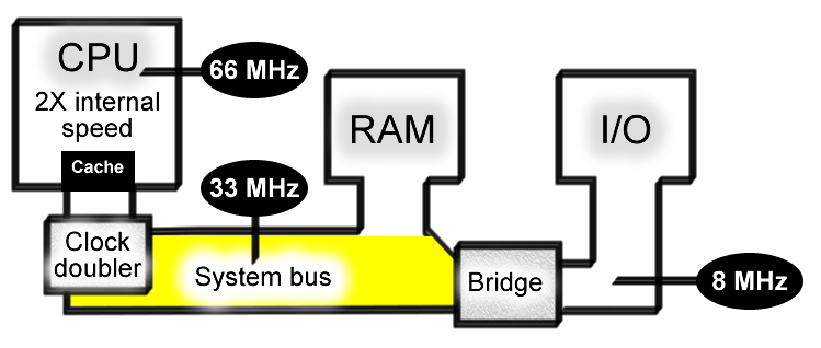 Fig. 120. The bus system for an 80486
processor.
Fig. 120. The bus system for an 80486
processor.
But this system places heavy demands on the RAM, because when the CPU internally processes twice as much data, it of course has to be fed more often. The problem is, that the RAM only works half as fast as the CPU.
For precisely this reason, the 486 was given a built-in L1 cache, to reduce the imbalance between the slow RAM and the fast processor. The cache doesnt improve the bandwidth (the RAM doesnt work any faster), but it ensures greater efficiency in the transfer of data to the CPU, so that it gets the right data supplied at the right time.
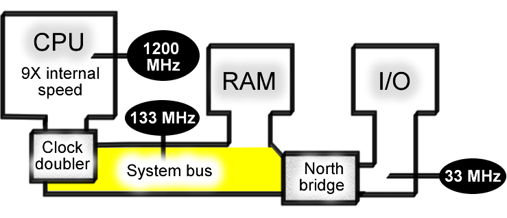
Clock doubling made it possible for Intel to develop processors with higher and higher clock frequencies. At the time the Pentium was introduced, new RAM modules became available, and the system bus was increased to 66 MHz. In the case of the Pentium II and III, the system bus was increased to 100 and 133 MHz, with the internal clock frequency set to a multiple of these.