Copyright Michael Karbo and ELI Aps., Denmark, Europe.
Chapter 20. RAM technologies
Lets look a little more closely at the technology which is used in the various types of RAM.
In the old days
Back in the 1980s, DRAM was used. This was dynamic RAM, which was relatively slow. It was replaced by FPM (Fast Page Mode) RAM which was also dynamic, only a bit faster.
Originally, loose RAM chips were installed directly in large banks on the motherboard. Later people started combining the chips in modules. These came in widths of 8 bits (with 30 pins) and 32 bits (with 72 pins). The 32-bit modules were suited to the system bus for the 80486 processor, which was also 32 bits wide.
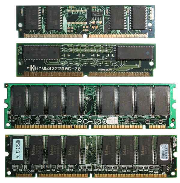 Fig. 135. Older RAM modules.
FPM RAM could not run any faster than 66 MHz, but that was fine for the system bus clock frequency in the original Pentium processors.
After FPM
came EDO RAM (Extended Data Out).
When Intel launched the Pentium processor, there was a change to using the 64 bit wide RAM modules (with 168 pins, as in Fig. 127 on page 51, which are still used for SDRAM today.
 Fig. 136. An old motherboard with sockets
for both 64-bit and 32-bit RAM modules. From the transition period between
Fig. 136. An old motherboard with sockets
for both 64-bit and 32-bit RAM modules. From the transition period between SDRAM
The big qualitative shift came in around 1997, when SDRAM (Synchronous DRAM) began to break in. This is a completely new technology, which of course required new chipsets. SDRAM, in contrast to the earlier types of RAM, operates synchronously with the system bus.
Data can (in burst mode) be fetched on every clock pulse. Thus the module can operate fully synchronised with (at the same beat as) the bus without so-called wait states (inactive clock pulses). Because they are linked synchronously to the system bus, SDRAM modules can run at much higher clock frequencies.
The 100 MHz SDRAM (PC100) quickly became popular, and with new processors and chipsets, the speed was brought up to 133 MHz (PC133).
Another innovation in SDRAM is the small EEPROM chip called the Serial Presence Detect chip, which is mounted on the modules. It is a very small chip containing data on the modules speed, etc.
 Fig. 137. The motherboard BIOS can now read
SDRAM module specifications directly.
Fig. 137. The motherboard BIOS can now read
SDRAM module specifications directly.
DDR RAM
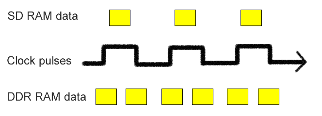
It is expensive to produce fast RAM chips. So someone hit on a smart trick in 1999-2000, which in one blow made normal RAM twice as fast. That was the beginning of DDR RAM (Double Data Rate). See the module in Fig. 131.
In DDR RAM, the clock signal is used twice. Data is transferred both when the signal rises, and when it falls. This makes it possible to perform twice as many operations per clock pulse, compared to earlier RAM types:
Timings
DDR RAM exist in many versions, with different the clock frequencies and timings. The timing indicates how many clock cycles there are wasted, when the motherboard waits for the memory to deliver the requested data.
With smaller numbers, we have better timings and the CPU having fewer idle clock cycles. You may find memory modules of the same clock frequency but with different timings. The better timing, the more expensive the RAM module is.
Ordinary pc users need not to speculate in special RAM with fast timing; this is primary sold to gamers and over-clockers, who tries to achieve the maximum performance from their motherboards.
|
Module |
Clock frequency |
Timing |
|
PC2100 |
2 x 133 MHz |
2-2-2 |
|
PC 2700 |
2 x 166 MHz |
2-2-2 |
|
PC 3200 |
2 x 200 MHz |
2-3-2 |
|
PC 3700 |
2 x 233 MHz |
3-4-4 |
|
PC 4000 |
2 x 250 MHz |
3-4-4 |
|
PC 4400 |
2 x 275 MHz |
3-4-4 |
Note that different timing means that the gain in terms of increased bandwidth doesnt quite match the clock speed. It is a bit less.
Next generation RAM
In the beginning the problem with DDR RAM, was that the RAM modules were poorly standardized. A module might work with a particular motherboard, but not with another. But this which was typical for a new technological standard is not a big problem anymore. Intel was initially against DDR RAM. They claimed that Rambus was a much better design, and that they wouldnt use DDR RAM. But consumers wanted DDR RAM, which Intels competitors were able to deliver, and in the end even Intel had to give in. At the end of 2001, the i845 chipset was released, which uses DDR RAM for the Pentium 4, and later we had the i865 and i875 chip sets, which use dual channel DDR RAM.
The next generation of RAM is the DDR2, which is a new and better standardized version of DDR using less power. The DDR2 modules operates at higher clock speeds due to better design with higher signal integrity and a more advanced internal data bus. The first chip sets to use DDR2 was Intels i915 and i925. Later DDR4 is expected with clock frequencies of up to 1,6 GHz!
Rambus RAM
Rambus Inc., as already mentioned, has developed a completely new type of RAM technology. Rambus uses a completely different type of chip, which are mounted in intelligent modules that can operate at very high clock frequencies. Here is a brief summary of the system:
Rambus RAM thus has a completely new and different design. The modules are only 16 bits wide. Less data is transferred per clock pulse, but the clock frequencies are much higher. The actual Rambus modules (also called RIMM modules) look a bit like the normal SDRAM modules as we know them. They have 184 pins, but as mentioned, the ships are protected by a heat-conducting casing:
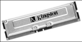
As the advanced Rambus modules are quite costly to produce, the technology is on its way out of the market.