Copyright Michael Karbo and ELI Aps., Denmark, Europe.
Chapter 36. Chipsets and hubs
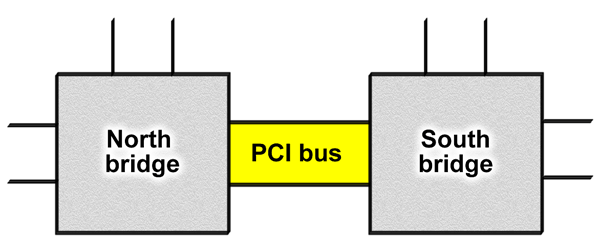
Since 1997, there has been more and more focus on refinement of the chipset, and not least the north bridge, which looks after data transfer to and from RAM. The south bridge has also been constantly developed, but the focus has been on adding new facilities.
For the north bridge, the development has focused on getting more bandwidth between the RAM and CPU. Lets look at a few examples of this.
Bridge or Hub
In a Pentium II motherboard, the I/O bus is directly linked to the system clock. The I/O bus (that is, in practise, the PCI bus) runs at 33 MHz, and that is typically a third or a quarter of the system clock speed (see Fig. 121).
In 1998-99, new developments took place at both AMD and Intel. A new architecture was introduced based on a Memory Controller Hub (MCH) instead of the traditional north bridge and an I/O Controller Hub (ICH) instead of the south bridge. I am using Intels names here; the two chips have other names at AMD and VIA, but the principle is the same. The first Intel chipset with this architecture was called i810.
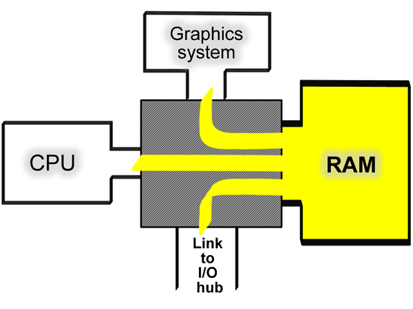
The MCH is a controller located between the CPU, RAM and AGP. It regulates the flow of data to and from RAM. This new architecture has two important consequences:
The new architecture is used for both Pentium 4 and Athlon processors, and in chipsets from Intel, VIA, and others. In reality, it doesnt make a great deal of difference whether the chipset consists of hubs or bridges, so in the rest of the guide I will use both names indiscriminately.
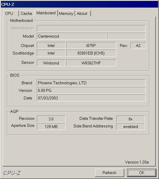
The i875P chipset
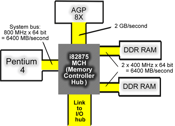
In 2003, Intel launched a chipset which work with the Pentium 4 and dual channel DDR RAM, each running at 200 MHz. This chip set became very popular, since it had a very good performance.
Another new feature in this chip set is that a Gigabit Ethernet controller can have direct access to the MCH (the north bridge). Traditionally the LAN controller is connected to the PCI bus. But since a gigabit network controller may consume a great band width, it is better to plug it directly into north bridge. This new design is called Communication Streaming Architecture (CSA).
The i925 chipset
In late 2004 Intel introduced a new 900-series of chipsets. They were intended for the new generation of Pentium 4 and Celeron processors based on the LGA 775-socket (as in Figur 112. The chip sets comes with support for the PCI Express bus, which is replacing the AGP bus and with support of DDR2 RAM:
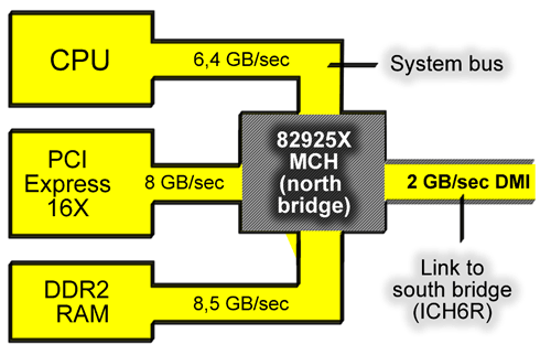
By making use of dual channel DDR2 RAM, a bandwidth of up to 8.5 GB/sec is achieved.
Big bandwidth for RAM
One might be tempted to think that the bandwidth to the RAM ought to be identical with that of the system bus. But that is not the case. It would actually be good if it was higher. Thats because the RAM doesnt only deliver data to the CPU. Data also goes directly to the graphics port and to and from the I/O devices bypassing the CPU. RAM therefore needs even greater bandwidth. In future architectures we will see north bridges for both Pentium 4 and Athlon XP processors which employ more powerful types of RAM, such as 533 MHz DDR2.