Answer: The answer is in red in the figure below.
Answer: 4 -- If you number the states, you should come up with a list going from 0 to 8. And what is 8 in binary? 1000. Since it takes 4 bits to represent 8, then four flip-flops are going to be required to remember 9 distinct states. Another way of looking at it is that 1 flip-flop can remember 21=2 states, 2 flip-flops can remember 22=4 states, 3 flip-flops can remember 23=8 states, and 4 flip-flops can remember 24=16 states. 1, 2, and 3 are not enough. Four is the first value that has more than 9 possible states.
Answer:
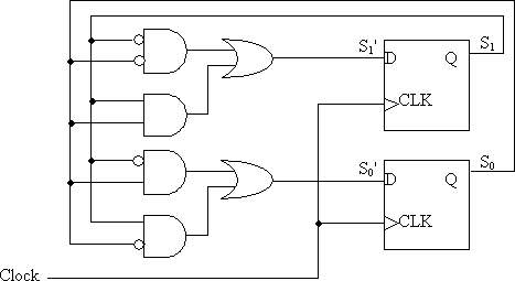
| Next State Table | |||||
| Current State | Next State | ||||
| S2 | S1 | S0 | S2' | S1' | S0' |
| 0 | 0 | 0 | 1 | 1 | 0 |
| 0 | 0 | 1 | 0 | 0 | 0 |
| 0 | 1 | 0 | 0 | 1 | 1 |
| 0 | 1 | 1 | 1 | 0 | 1 |
| 1 | 0 | 0 | 0 | 0 | 1 |
| 1 | 0 | 1 | 1 | 1 | 1 |
| 1 | 1 | 0 | 0 | 1 | 0 |
| 1 | 1 | 1 | 1 | 0 | 0 |
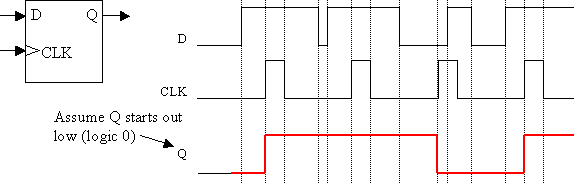
Answer: If the current state is 01 and D=0, then after a clock pulse, the state machine will head to state 10. The output for that state is 0.
Answer: S0' = (S0 ^S1) + (^S0 S1)
S1' = (^S0 ^S1) + (S0 S1)
Answer:
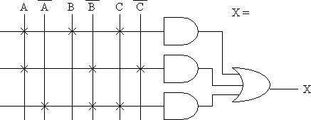
Answer: X = (A B C) + (A ^B ^C) + (^A ^B C)
Answer: From the circuit, we can see that S2=0, S1=1, and S0=1. Since we assume that S2 is the considered the most significant bit, then the selection inputs make the binary value 0112. This is equivalent to the decimal value 3. Therefore, D3 (which is equal to 0) is routed to the output Y. The final answer (the only thing that you actually needed to write down for full credit) is 0.
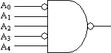
Answer: An active low decoding logic, otherwise known as a chip select circuit, is created using a NAND gate where the inputs that are supposed to equal 0 are inverted before being input to the NAND gate and the inputs that are supposed to equal 1 are connected straight into the NAND gate. This gives us the following circuit:
Answer: This state, identified in class as Z, is called high-impedance. It is designed to disconnect the outputs of an IC such as a memory chip so that it is not trying to put a logic 1 or 0 on a wire while another chip is supposed to be controlling the wire. It is almost like a switch that physically disconnects an output from a circuit.
- Battery-backed SRAM
- Flash RAM
- Custom-masked ROM
- EEPROM
- OTPROM
- EPROM
Answer: a, b, c, d, e, and f (all of them)
- Battery-backed SRAM
- Flash RAM
- DRAM
- EEPROM
- OTPROM
- EPROM
Answer: e and f (d can be programmed with a programmer, but it is not required)
- Battery-backed SRAM
- Flash RAM
- Custom-masked ROM
- EEPROM
- OTPROM
- EPROM
Answer: a, b, d, and f
Answer: Since 217 = 128K (131,072), then the processor must have 17 address lines.
Answer: First, we need to determine how many address lines it will take to address 16K. Since 214 = 16K (16,384), then it takes 14 address lines. Therefore, the the 14 least significant places in the low or starting address MUST be zero. Therefore, we next convert 3C00016 to binary and get 0011 1100 0000 0000 00002. Counting from the right, we see that there are 14 zeros before you get to the first 1. Therefore, a 16K memory chip can have a starting address of 3C00016.
Answer: Once again, we need to figure out how many address lines an 8K memory device requires. Since 213 = 8K (8,192), then an 8K device has 13 address lines. Therefore, the 13 least significant or 13 rightmost bits of the address range for an 8K ROM must be 0's for the low address and 1's for the high address. Since our low address is 400016 which equals 0100 0000 0000 00002 in binary, then the low address is 0101 1111 1111 11112 (simply 0100 0000 0000 00002 where the last 13 bits have been changed to 1's). In hex, this is 5FFF16.
Answer: First, how many address lines will a 32K memory device require? Well, since 215 = 32K (32,768), then it requires 15 address lines.
Next, we need to figure out how many address lines total come from the processor to make a 1 MEG memory space. Since 220 = 1 MEG (1,048,576), then the processor has 20 address lines, A0 through A19.
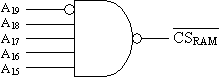
Third, we need to determine the bits required for the chip select. Begin by converting the low address of the memory device to binary: 7800016 = 0111 1000 0000 0000 00002. (Note that the leading zero was added because the processor has 20 address lines.) Since 32K requires 15 address lines, then the remaining lines, 20-15=5, will be used for the chip select. This means that the 5 most significant address lines, A19, A18, A17, A16, and A15, will make up the chip select.
From the binary value for the low address, we see that A19=0, A18=1, A17=1, A16=1, and A15=1. This gives us the circuit: