Answer:
| Inputs | Outputs | ||
| ^S | ^R | Q | ^Q |
| 0 | 0 | illegal | |
| 0 | 1 | 1 | 0 |
| 1 | 0 | 0 | 1 |
| 1 | 1 | Q0 | ^Q0 |
Answer: d) changing from a 0 to a 1 (rising edge).
Answer:
Answer:
|
|
P |
|
||
|
|
|
|
|
|
|
|
|
|
|
|
|
|
|
|
|
|
|
|
|
|
|
|
|
|
|
|
|
|
|
|
|
|
|
|
|
|
|
|
|
|
|
|
|
|
|
|
|
|
|
|
|
|
Answer:
Answer:
It is impossible to get to state "three". Since it is impossible to get to the state, it has no place in the state diagram.
Answer:
First, you must understand that 42 states must be represented with 42 different binary values, i.e., the binary equivalents of 0 through 41. Once you know this, there are a couple of ways to do this. You can convert 41 to binary and get 1010012. After you get rid of any leading zeros, you should see that this number requires 6 binary digits. Therefore, it takes 6 flip-flops to represent the states of a state machine with 42 states.
The second way to do this is to look at the powers of two and find where 42 falls.
|
|
|
|
|
|
|
|
|
|
|
|
|
|
|
|
|
|
|
|
|
Since 42 lies between 32 and 64, then the number of flip-flops required equals the power that 2 is raised to for the upper limit of 64. Once again, this is 6.
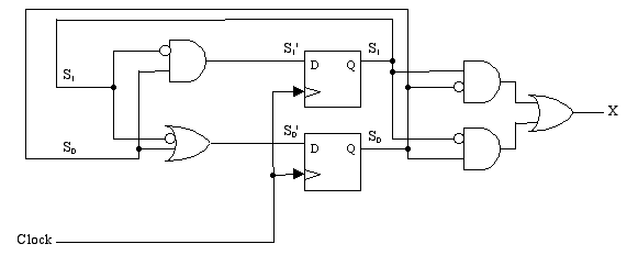
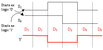
S0' = S0 + ^S1
S1' = ^S1 S0
X = ^S1 S0 + ^S0 S1
Answer:
Answer:
Answer:
The inputs to the decoder act as a channel selector determining which of the outputs receives the "active low" output. Since the inputs to the decoder (in order of significance) are 101, and since the decimal equivalent of 101 is 5, then output D5 equals zero. All of the other outputs equal 1.
Answer: Since there are 24 address lines, then there must be 224 different addresses or rows. Since there are 16 data bits (columns) per address, then the answer is 224 * 16.
Answer: To be faster.
Answer:
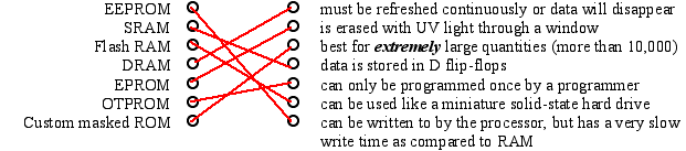
Answer: False -- The capacitors that make up a DRAM are far cheaper than flip-flops.
Answer: True -- The capacitors that make up a DRAM are far smaller than flip-flops and therefore more can be packed into the same space.
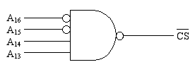
Answer: Examining the circuit reveals that to have the chip select go to zero, the address values must be A15 = 0, A14 = 0, A13 = 1, A12 = 0, and A11 = 1.
|
|
|
|
|
|
|
|
|
|
|
|
|
|
|
|
|
|
|
|
|
|
|
|
|
|
|
|
|
|
|
|
|
|
The low address should have 0's in all of the positions where X's are in the table above and the high address should have 1's. Therefore, the low address should be:
|
|
|
|
|
|
|
|
|
|
|
|
|
|
|
|
|
|
|
|
|
|
|
|
|
|
|
|
|
|
|
|
|
|
Converting to hex we get a low address of 280016.
The high address should be:
|
|
|
|
|
|
|
|
|
|
|
|
|
|
|
|
|
|
|
|
|
|
|
|
|
|
|
|
|
|
|
|
|
|
Converting to hex we get a high address of 2FFF16.
Answer: The size of the section of memory reserved by a chip select is determined by the number of bits that are allowed to change from 0 to 1 in the range. In problem 16, bits A0 through A10 are allowed to change, 11 bits. Therefore, the size of the section of memory reserved by the chip select.
Size of memory = 211 = 2K
Answer: The answer can be found one of two ways. First, you can figure out the size of the processor's memory space (dictated by the 27 address lines), then divide 128K into that.
227 = 128 Meg
128 Meg/128K = 1024 times
The other way is to figure out how many lines are left for the chip select after taking out the address lines for the 128K memories. Since 128K takes 17 address lines, then 27 - 17 = 10 lines are left. That means we can have 210 = 1024 different chip select circuits.
Answer: False
First, convert each of these addresses into binary.
| Address bits: |
|
|
|
|
|
|
|
|
|
|
|
|
|
|
|
|
| Low address: |
|
|
|
|
|
|
|
|
|
|
|
|
|
|
|
|
| High address: |
|
|
|
|
|
|
|
|
|
|
|
|
|
|
|
|
Can we draw a line where both the high and the low address have EXACTLY the same bits to the left of the line and the low address has all zeros to the right and the high address has all ones?
Well, if we draw the line between bits 10 and 11, then bit 9 doesn't follow the requirement where all the bits of the low address must be 0 to the right of the line. If we draw the line between bits 9 and 8, then all of the bits to the left of the line do not stay the same for the low and the high addresses.
Therefore, since we can't draw this line, there is no way that these addresses can be the high and low limits of a single chip select.
Answer: True
To determine the answer to this problem, we need to begin by figuring out how many bits the 2K memory needs for its own address lines. Since 211 = 2K, then we know that 11 address lines will be needed. Now we need to figure out if the low address above has its 11 least significant bits set to zero. (That allows the address to follow the rules outlined in problem 19.)
|
|
|
|
|
|
|
|
|
|
|
|
|
|
|
|
|
|
|
|
|
|
|
|
|
|
|
|
|
|
|
|
|
|
|
|
|
|
|
|
|
|
Counting from the right side of this binary value, we count eleven zeros before we encounter our first 1. Therefore, this address can be the low address of a 2K chip select.
Answer: