Parameterized word length and depth
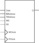
Dual port synchronous RAM architecture
Dual port synchronous write, asynchronous read RAM architecture
3200DX, MX
The RAM cores use 3200DX and MX, 32x8 or 64x4, dual port RAM cells.
In the synchronous mode, the read and write operations are totally independent and can be performed simultaneously. The operation of the RAM is fully synchronous with respect to the clock signals, WClock and RClock. Data of value Data are written to the WAddress of the RAM memory space on the rising (RISE) or falling (FALL) edge of the clock WClock (WCLK_EDGE). Data are read from the RAM memory space at RAddress into Q on the rising (RISE) or falling (FALL) edge of the clock signal RClock (RCLK_EDGE).
The behavior of the RAM is unknown if you write and read at the same address and signals WClock and RClock are not the same. The output Q of the RAM depends on the time relationship between the write and the read clock.
In the asynchronous mode, the operation of the RAM is only synchronous with respect to the clock signal WClock. Data of value Data are written to the WAddress of the RAM memory space on the rising (RISE) or falling (FALL) edge of the clock signal WClock (WCLK_EDGE). Data are read from the RAM memory space at RAddress into Q after some delay when RAddress has changed.
The behavior of the RAM is unknown if you write and read at the same address. The output Q depends on the time relationship between the write clock and the read address signal.
The WIDTH (word length) and DEPTH (number of words) have continuous values but the choice of WIDTH limits the choice of DEPTH and vice versa.
The write enable (WE) and read enable (RE) signals are active high request signals for writing and reading, respectively; you may choose not to use them.
|
Port Description |
|
Port Name |
Size |
Type |
Req/Opt |
Function |
|
Data |
WIDTH |
input |
Req. |
Input Data |
|
WE |
1 |
input |
Opt. |
Write Enable |
|
RE |
1 |
input |
Opt. |
Read Enable |
|
WClock |
1 |
input |
Req. |
Write clock |
|
RClock |
1 |
input |
Opt. |
Read clock |
|
Q |
WIDTH |
output |
Req. |
Output Data |
|
Parameter Description |
|
Parameter |
Value |
Function |
|
WIDTH |
width |
Word length of Data and Q |
|
Depth |
depth |
Number of RAM words |
|
WE_POLARITY |
1 2 |
WE can be active high or not used |
|
RE_POLARITY |
1 2 |
RE can be active high or not used |
|
WCLK_EDGE |
RISE FALL |
WClock can be rising or falling |
|
RCLK_EDGE |
RISE FALL NONE |
RClock can be rising, falling, or not used |
|
Implementation Parameters |
|
Parameter |
Value |
Description |
|
LPMTYPE |
LPM_RAM_DQ |
Generic Dual Port RAM category |
|
Fan-in Parameters |
|
Parameter |
Value |
Description |
|
RAMFANIN |
AUTO MANUAL |
See Fan-In Control section below |
|
Parameter Rules |
|
Parameter Rules |
|
If RCLK_EDGE is NONE (Asynchronous mode), then RE_POLARITY must be 2 (note used) |
|
The number of RAM blocks used (function of width and depth) must be less than or equal to the number of RAM blocks in one column of the largest device. |
One of the key issues when building RAM cores is control of the routing congestion near the RAM cells. The problem becomes more critical when deep RAM cores are built. You need to broadcast signals throughout the height of the chip. The place-and-route algorithm could have difficulties satisfying all routing constraints. As a result, much slower routing resources could be allocated to satisfy all constraints. To make this problem less likely, a special buffering scheme has been implemented to relieve the congestion near the RAM cells. However, you may choose to control the buffering yourself to improve performances when needed. The RAM core can be built using either the automatic buffering architecture or the manual buffering architecture.
In this mode (default), a buffering scheme is automatically built into the RAM core architecture (see the figure below). This mode should always be considered first. However, if the performance is not met, it may be better to use the manual buffering option.
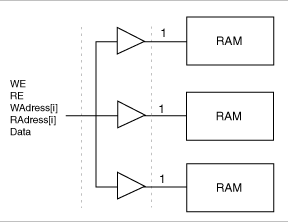
Automatic Buffering for RAM cores
The figure below (Manual Buffering) shows how manual buffering is executed. A fan-in of one (1) is enforced on all signals fanning out to more than one RAM cell. If these signals were broadcast to all RAM cells, very slow routing resources (long freeways) would be required to route the signals impacting the RAM performance.
Manual buffering should only be used if the expected performance is not realized using the automatic buffering scheme, or if you know ahead of time that you need to use this scheme to meet your timing goals. In this architecture, the idea is not to buffer the signals internally but rather give some kind of access to the RAM core internal signals. Then, you must buffer the signals outside the core and either use traditional buffers or duplicate the logic that drives these signals externally. If you choose manual buffering, the WE, RE, Waddress(i), RAddress(i), and Data[i] signals become busses external to the core. For all these signals, the bus width is equal to the number of RAM cells (used to build a given configuration) driven by each signal. The Manual Buffering figure below illustrates the manual buffering architecture for a 96x8 RAM configuration, built of three 32x8 configured RAM cells. In this configuration, the WE, RE, WAddress and RAddress signals drive all RAM cells simultaneously. The Manual Buffering for the Data Bus shows a 128x8 RAM configuration, built using four 64x4 configured RAM cells. In that configuration, the 8-bit data bus is split into two completely independent 4-bit data busses.
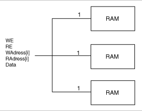
Manual Buffering (96x8 RAM Configuration)
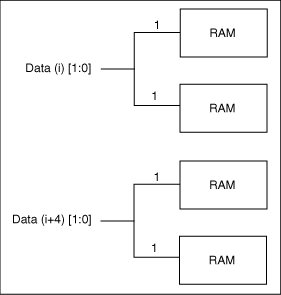
Manual Buffering for the Data Bus (128x8 RAM Configuration)
Timing waveforms for this core are available in the SmartGen Cores Reference Guide. The reference guide is located in the designer\doc directory on the hard drive where you installed your Actel Libero IDE or Designer software.