Clock Delay Adjustment
Clock Frequency Synthesis
Clock phase shifting
APA
|
Parameter |
Value |
Function |
|
CLKS |
1 2 |
Primary or Both outputs |
|
FIN |
1.5 - 180 MHz |
Input Frequency |
|
PRIMFREQ |
1.5 - 240 MHz |
Primary Output Frequency |
|
PDELAYVAL |
0 - 8 ns |
Primary Delay value, in steps of .25 ns |
|
PDELAYSIGN |
0 1 |
Positive or Negative primary delay |
|
PPHASESHIFT |
0 90 180 270 |
Primary Phase-shift |
|
PBYPASS |
0 1 |
No Yes. Primary Bypass |
|
FIN2 |
1.5 - 240 MHz |
Secondary Input Frequency, Only if PLL is bypassed for Secondary Output |
|
SECFREQ |
1.5 - 240 MHz |
Primary Output Frequency |
|
SDELAYVAL |
0 - 8 ns |
Primary Delay value, in steps of 0.25 ns A |
|
SDELAYSIGN |
0 1 |
Positive or Negative primary delay |
|
SPHASESHIFT |
0 90 180 270 |
Primary Phase-shift |
|
SBYPASS |
0 1 |
No Yes. Primary Bypass |
|
FB |
Internal Deskewed |
Feedback |
|
CONF |
STATIC DYNAMIC |
Configuration |
|
A. In the GUI, the delay is entered directly as a value between -3.75 and +3.75 without breaking it into sign and value. |
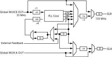
Schematic of the ProASICPLUS PLL; example shows 33 MHz in, 133 MHz out
Summary of the menu items available when you generate a PLL for ProASICPLUS.
Configuration - Dynamic or Static Configuration
In dynamic mode, designers are able to set all the configuration parameters using either the external JTAG port or an internally-defined serial interface. The dynamic-mode PLL can be switched to static mode during operation by just changing a mode selection bit. This way you can have one stable static configuration, yet for selected sequences of events, you can switch to dynamic mode and run the clock at a different frequency if required. For the Dynamic mode, SmartGen is used to specify a stable default configuration.
Input Clock Frequency - Floating point value between 1.5 and 180 MHz
Primary Clock Frequency - Floating point value between 1.5 and 180 MHz. If the specified frequency cannot be achieved, the closest approximate frequency will be provided. There are some restrictions on the possible values of this frequency even in the specified range, based on the PLLCORE limitations. SmartGen takes all these limitations into consideration when generating a PLL. If the specified frequency cannot be achieved, the closest approximate frequency will be provided.
Bypass PLL in Primary Clock - Selecting this check box bypasses the PLL for the primary clock. This feature enables you to bypass the PLLCORE functionality and use the surrounding divider and delay elements. When the PLL is bypassed, the primary clock frequency must be equal to or be 1/2, 1/3 or ¼ of input frequency, as only a divider is available in the output path.
Primary Clock Phase Shift - Supports four values 0, 90, 180, and 270 degrees. Not valid when PLL is bypassed for primary clock. The secondary clock cannot be phase-shifted.
Selecting a phase shift of 90 degrees and an output divider other than 1 causes SmartGen to return a message about the actual phase shift being 90 divided by the divider.
Primary Clock Delay - This is a floating point between -4.0 and 8.0 with increments of 0.25. When PLL is bypassed for primary clock, only 0, 0.25, 0.5 and 4 ns are valid delays.
Secondary Clock Input Frequency - Floating point value between 1.5 and 240 MHz. This is valid only when secondary clock is selected and PLL is bypassed.
Secondary Clock Output Frequency - Floating point value between 1.5 and 240 MHz. This is valid only when secondary clock is selected. If the specified value cannot be achieved, the closest approximate frequency will be provided.
Bypass PLL in Secondary clock - Selecting this check box bypasses the PLL for secondary clock. When the PLL is bypassed, the secondary clock frequency must be equal to or be 1/2, 1/3 or ¼ of secondary input frequency. This feature allows the user to bypass the PLLCORE functionality and use the surrounding divider and delay elements.
Secondary Clock Delay - This is a floating point between -4.0 and 8.0 with increments of 0.25. When PLL is bypassed for secondary clock, only 0, 0.25,0.5 and 4 ns are the valid delays.
Feedback - A radio button to select between Internal, External, and Deskewed feedback.
The clock-conditioning circuitry enables you to implement the feedback clock signal using either the output of the PLL, an internally generated clock, or an external clock. When external feedback is selected, an additional port, EXTFB, is made available to the user to drive the feedback. The internal feedback signal can be further delayed by a fixed amount designed to emulate the delay through the chip’s clock tree. This allows for clock-line de-skewing operations. This delay is included in the feedback path when deskewed feedback is chosen. This value is dependent on the device you are using.
|
Port Description |
|
Name |
Size |
Type |
Req/Opt |
Function |
|
GLA |
1 |
Output |
Opt |
Secondary clock output |
|
GLB |
1 |
Output |
Req |
Primary clock output |
|
LOCK |
1 |
Output |
Req |
PLL Lock |
|
SDOUT |
1 |
Output |
Req |
Output of serial interface shift register |
|
CLK |
1 |
Input |
Req |
Input clock for primary clock |
|
CLKA |
1 |
Input |
Opt |
Input clock for secondary clock. Valid only in Bypass Mode |
|
EXTFB |
1 |
Input |
Opt |
External Feedback |
|
SCLK |
1 |
Input |
Opt |
Shift Clock (Only Dynamic Mode) |
|
SSHIFT |
1 |
Input |
Opt |
Serial Shift enable (Only Dynamic Mode) |
|
SDIN |
1 |
Input |
Opt |
Serial Data in for PLL configuration bits (Only Dynamic Mode) |
|
SUPDATE |
1 |
Input |
Opt |
Serial Update (Only Dynamic Mode) |
|
MODE |
1 |
Output |
Opt |
Dynamic or Static mode indicator |
For more detailed information and more schematics of the APA PLL, please refer to Using ProASICPLUS Clock Conditioning Circuits,the ProASICPLUS PLL Dynamic Reconfiguration Using JTAG, and the ProASICPLUS Datasheet (http://www.actel.com/documents/ProASICPlusDS.pdf) at http://www.actel.com.