Parameterized word length and depth
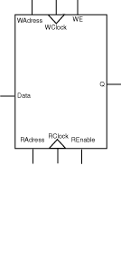
Dual-port synchronous RAM architecture
Dual-port synchronous write, asynchronous read RAM architecture
Write and read enable
Behavioral simulation model in VHDL and Verilog
SX, SX-A, eX
The register file is a core unique to the SX, SX-A, and eX families. This core synthesizes the equivalent of small RAM blocks using ordinary logic, thereby making memory cells available to you even though the silicon does not explicitly have hardware support for RAM.
In synchronous mode, the read and write operations are totally independent and can be performed simultaneously. The operation of the register is fully synchronous with respect to the clock signals WClock and RClock. Data of value Data are written to the WAddress of the register memory space on the rising (RISE) or falling (FALL) edge of the clock WClock (WCLK_EDGE). Data are read from the register memory space at RAddress into Q on the rising (RISE) or falling (FALL) edge of the clock RClock (RCLK_EDGE).
The behavior of the Register is unknown, if designers write and read at the same address and WClock and RClock are not the same. The output Q of the register depends on the time relationship between the write and the read clock.
In asynchronous mode, the operation of the register is only synchronous with respect to the clock signal WClock. Data of value Data are written to the WAddress of the register memory space on the rising (RISE) or falling (FALL) edge of the clock WClock (WCLK_EDGE). Data are read from the register memory space at RAddress into Q after some delay when RAddress has changed.
The WIDTH (word length) and DEPTH (number of words) have continuous values but the choice of WIDTH limits the choice of DEPTH and vice versa.
The write enable (WE) and read enable (RE) signals are active high request signals for writing and reading, respectively. You may not utilize them.
|
Port Description |
|
Port Name |
Size |
Type |
|
Data |
WIDTH |
input |
|
WE |
1 |
Input |
|
RE |
1 |
Input |
|
WClock |
1 |
Input |
|
RClock |
1 |
Input |
|
Q |
WIDTH |
Output |
|
Parameter Description |
|
Parameter |
Value |
Function |
|
WIDTH |
Width |
Word length of Data and Q |
|
DEPTH |
Depth |
Number of RAM words |
|
WE_POLARITY |
1 2 |
WE can be active high or not used |
|
RE_POLARITY |
1 2 |
RE can be active high or not used |
|
WCLK_EDGE |
RISE FALL |
WClock can be rising or falling |
|
RCLK_EDGE |
RISE FALL NONE |
RClock can be rising, falling, or not used |
|
|
|
|
|
Timing Waveform Terminology |
|
Term |
Description |
Term |
Description |
|
tckhl |
Clock high/low period |
tdsu |
Data setup time |
|
trp |
Reset pulse width |
trco |
Data valid after clock high/low |
|
twesu |
Write enable setup time |
trao |
Data valid after read address has changed |
|
tresu |
Read enable setup time |
tco |
Flip-flop clock to output |
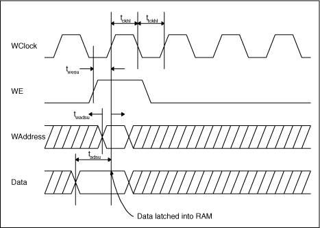
Ram Write Cycle
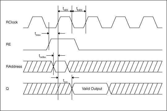
RAM Synchronous Read Cycle
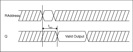
RAM Asynchronous Read Cycle