

|
|
| |
|
Answers Database
LogiCORE PCI32 4000: Verilog synthesis/simulation with PCI LogiCORE v2.0, FPGA Express v1.2, & M1.3.7
Record #3105
Product Family: Software ../source/ping_tb.v -testbench file ../source/stimulus.v -signal generation used in testbench ../source/dumb_target.v -signal generation used in testbench ../source/dumb_arbiter.v -signal generation used in testbench ../source/pcim_top.v -top-level Verilog file which connects core to ping ../source/ping.v -ping design(user applications) ../source/cfg.v -Used to configure features in the PCI LogiCORE v2.0 ../../src/xpci/pcim_lc.v -Verilog simulation model of the PCI LogiCORE v2.0../../src/xpci/pci_lc_i.v -Verilog simulation model of the PCI LogiCORE v2.0 For a user design, the ping.v file is replaced with the user Verilog code. At a minimum cfg.v, pcim_lc.v, and pci_lc_i.v must always be used. (3) Setup your Verilog simulator to point to the Verilog simulation library in M1.3.7. The Verilog simulation library is located at %XILINX%\verilog\data. (4) Functionally simulate the PCI LogiCORE v2.0 by processing the list of files in step (2) into the Verilog simulator. Solution 2: Timing Simulation with the PCI LogiCORE v2.0 and M1.3.7. (1) After place and route, a structural Verilog file, pcim_top_routed.v, and an SDF file, pcim_top_routed.sdf, will be in the c:\mypci directory. (2) Setup your Verilog simulator to use the M1.3.7 Verilog simulation libraries, which are located in %XILINX%\verilog\data. (3) Simulate the PCI LogiCORE design, by reading in the pcim_top_routed.v file, pcim_top_routed.sdf file, and testbench file into the Verilog simulator. In this case for the ping design, the 'testbench' is comprised of the following files: c:\pcim\verilog\example\source\ping_tb.v c:\pcim\verilog\example\source\stimulus.v c:\pcim\verilog\example\source\dumb_target.v c:\pcim\verilog\example\source\dumb_arbiter.v Solution 3: Synthesis/Place & Route of the PCI LogiCORE v2.0 with FPGA Express v1.2 and M1.3.7 (1) Asumming that 'pcim' is installed in your root directory, copy the following Verilog files into a directory of your choice. For this example, the directory is c:\mypci: copy c:\pcim\verilog\example\source\ping.v c:\mypci copy c:\pcim\verilog\example\source\cfg.v c:\mymci copy c:\pcim\verilog\example\source\pcim_top.v c:\mypci (2) Start FPGA Express and create a project in c:\mypci. (3) After creating the project, read in the files in the mypci directory into the FPGA Express project. 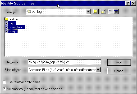 Figure 1- Read Verilog file into project 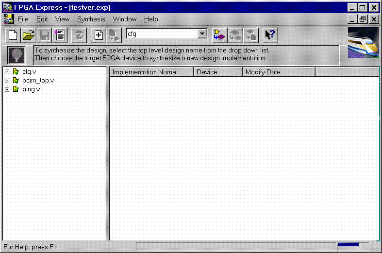 Figure 2- Verilog files analyzed (4) After the files have been 'analyzed', create an implementation. When the 'Create Implementation' window appears, set 'Family' to XC4000; set 'Device' to 4013xlpq208; set 'Speed grade' to -1. Check the box 'Do not insert I/O Pads'. 4013xlhq240-1 is also a valid part type for the PCI LogiCORE v2.0. (The PCI LogiCORE can also be used with the 4062xlpq208-1 or 4062xlhq240-1) 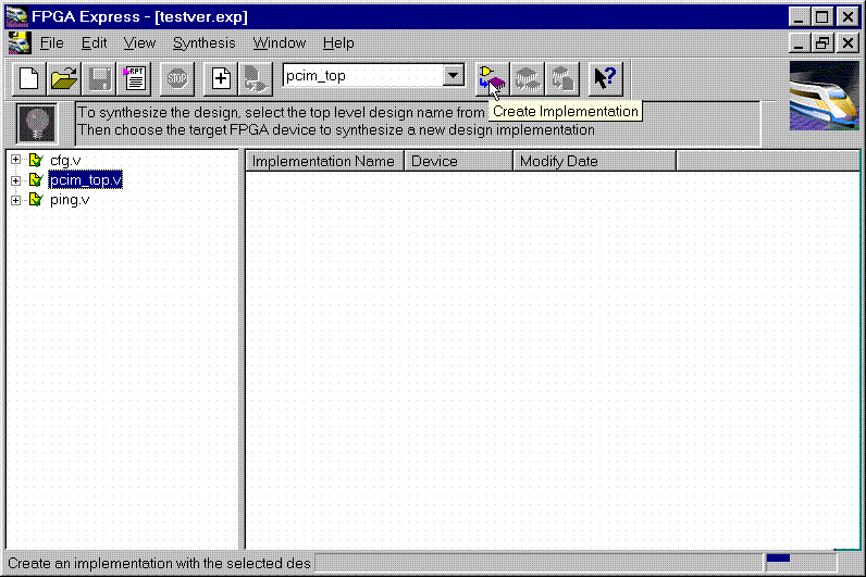 Figure 3- Implement the Design 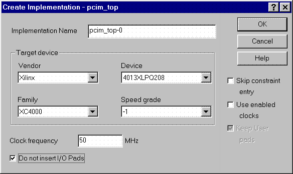 Figure 4- Create Implementation Window By default, FPGA Express v1.2 automatically inserts the correct I/O cells. The PCI LogiCORE v2.0 already has I/O inside of it. FPGA Express v1.2 can only insert all I/O cells or none at all. If FPGA Express was allowed to behave in its 'default' way, a syntactically incorrect netlist would be created. FPGA Express must be prevented for inserting I/O cells. I/O cells for the user application, in this case 'ping', must have the I/O cells instantiated manually. (5) Double-click on the implemenation that was created. A 5-tab window will appear. Select the 'Modules' tab. 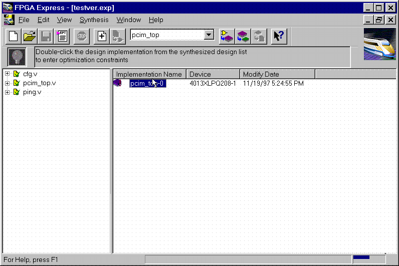 Figure 5- Open implementation 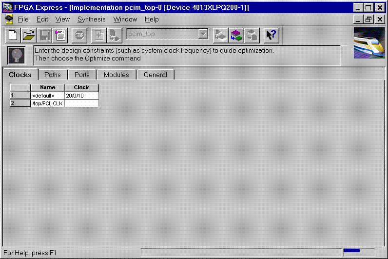 Figure 6- Implementation View (6) Under Modules, four items will be listed: IBUF, PCI_CORE, OBUF, and PING. Place a 'preserve' on all four items. 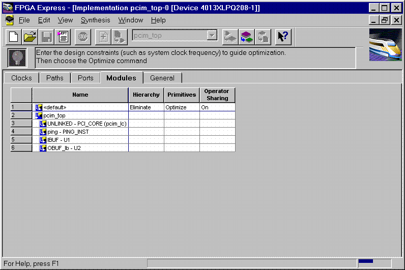 Figure 7- Implementation-Modules view For a user design, a preserve must always be placed on PCI_CORE, any instantiated I/O, and on the user application (in this case ping). 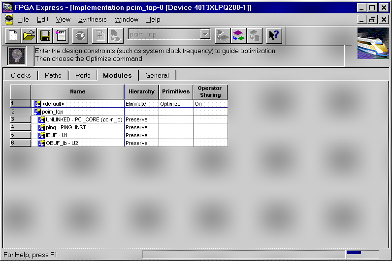 Figure 8- 'Preserve' attribute applied (7) Apply constraints in the implementation window as desired. Constraints can be applied via the 'Clock', 'Path', & 'Ports' tabs in the implementation window. (8) Close the implementation and 'optimize' (synthesize) the design. 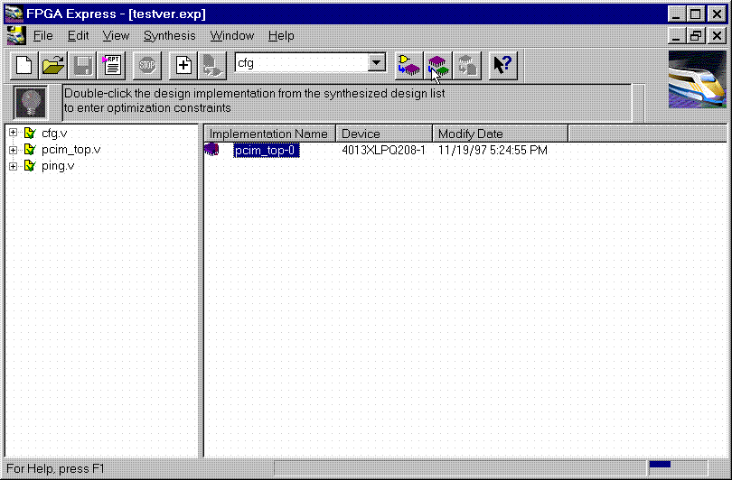 Figure 9- Optimize (9) An error may happen during optimization. Because FPGA Express v1.2 is instantiating a black-box, Express is unable to determine the correct pin directions for some of the pins of the core. Error messages of this type will appear as: 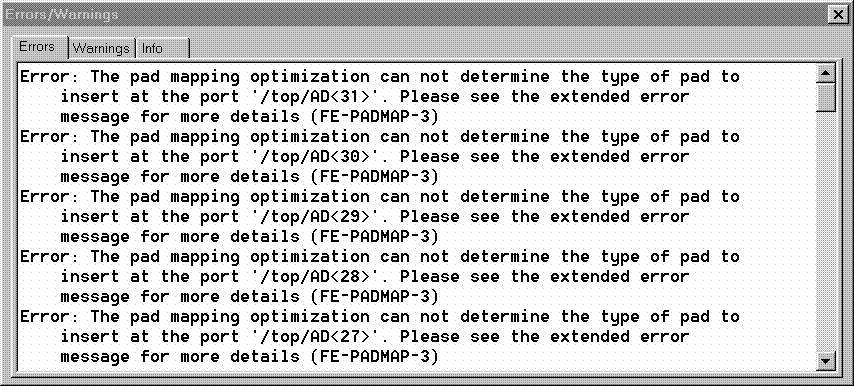 Figure 10- Error message on ports If this happens, the pad directions for the listed pins must be specified. Go back to the Implementation Window and select the 'Ports' tab. Based on the list of ports Express cannot determine direction, find those pins in the 'Ports' view and select that pin in the 'Pad' column. In this example, AD<31> is used. Select 'Define' for AD<31>. 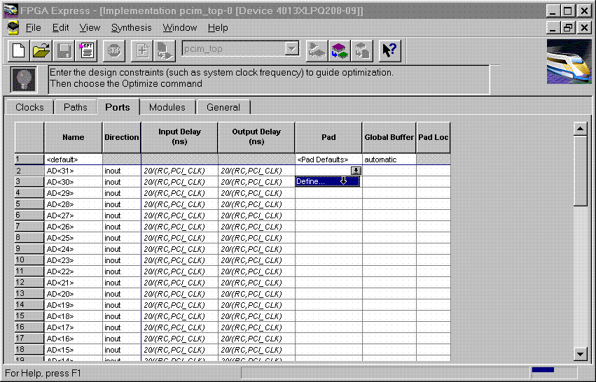 Figure 11- Defining port directions, part 1 The 'Define Pad' window will appear. Since AD is really an inout port, in the 'Pad Type' section of the 'Define Pad' window, select output. If the port was defined as an input, then input in 'Pad Type' would have been selected. If the port was defined as output, then output would have been selected in 'Pad Type'. 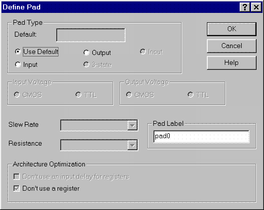 Figure 12- Defining port directions, part 2 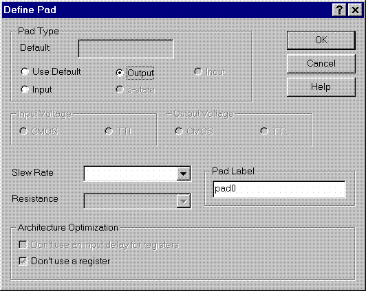 Figure 13- Defining port directions, part 3 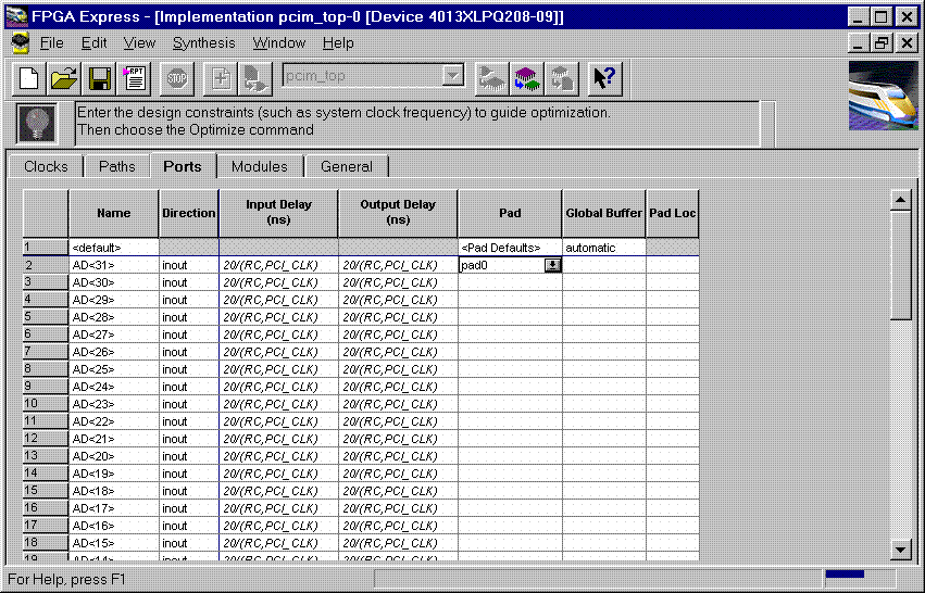 Figure 14- Defining port directions, part 4 Specify the pin direction for all ports listed in the error window during the optimize phase. Once a 'padn' has been defined, the padn direction can be copied for other ports of a similar type. 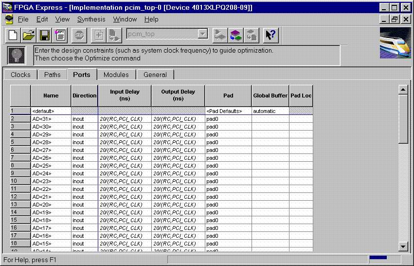 Figure 15- Defining port directions part 5 (10) Re-optimize the design. For future revisions, duplicate the implementation that contains the correct pad directions for the core. 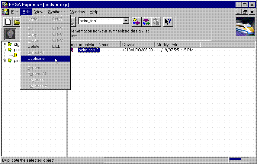 Figure 16- Duplicating the Implementation (11) If optimization is succesful, write out the XNF files for the design. Place the XNF files in the c:\mypci directory. Two XNF files will be produced by FPGA Express. One file will be named after the top-level design file (in this case pcim_top.xnf). The other file will be named after the user application (in this case ping.xnf). (12) Edit the top-level XNF file from FPGA Express v1.2 (in this case pcim_top.xnf). FPGA Express v1.2 is unable to determine the pin directions for the instantiated PCI LogiCORE v2.0. M1.3.7 is very strict in checking pin directions. The pin directions of the PCI LogiCORE v2.0 in the top-level XNF file from FPGA Express v1.2 must be edited. All the pin directions for the PCI LogiCORE in the pcim_top.xnf file will have the direction 'B'. PIN directions in a XNF file can be of three types: 'B', 'I', & 'O'. Edit the PIN directions for the SYM PCI_CORE only. The PIN directions for the PCI_CORE must correspond to the pin directions for the module pcim_lc. See the file c:\pcim\verilog\src\xpci\pcim_lc.v for the correct pin directions. Here is a partial example of what the PCI_CORE symbol will look like directly out of FPGA Express v1.2: LCANET, 6 PROG, FPGA Express, v1.2, Build 1.2.0.6.6.1997 PART, 4013EPQ208-1 SYM, PCI_CORE, pcim_lc, LIBVER=2.0.0 PIN, AD_IO<31>, B, AD<31>, , PIN, AD_IO<30>, B, AD<30>, , PIN, AD_IO<29>, B, AD<29>, , PIN, AD_IO<28>, B, AD<28>, , PIN, AD_IO<27>, B, AD<27>, , PIN, AD_IO<26>, B, AD<26>, , PIN, AD_IO<25>, B, AD<25>, , PIN, AD_IO<24>, B, AD<24>, , PIN, AD_IO<23>, B, AD<23>, , PIN, AD_IO<22>, B, AD<22>, , PIN, AD_IO<21>, B, AD<21>, , PIN, AD_IO<20>, B, AD<20>, , PIN, AD_IO<19>, B, AD<19>, , PIN, AD_IO<18>, B, AD<18>, , PIN, AD_IO<17>, B, AD<17>, , . . . . PIN, CFG<5>, B, KEEPOUT, , PIN, CFG<4>, B, KEEPOUT, , PIN, CFG<3>, B, KEEPOUT, , PIN, CFG<2>, B, KEEPOUT, , PIN, CFG<1>, B, KEEPOUT, , PIN, CFG<0>, B, C_READY, , PIN, PCI_RST, B, PCI_RST, , PIN, CLK, B, PCI_CLK, , END . . . The corrected PCI_CORE appears as follows: LCANET, 6 PROG, FPGA Express, v1.2, Build 1.2.0.6.6.1997 PART, 4013EPQ208-1 SYM, PCI_CORE, pcim_lc, LIBVER=2.0.0 PIN, AD_IO<31>, B, AD<31>, , PIN, AD_IO<30>, B, AD<30>, , PIN, AD_IO<29>, B, AD<29>, , PIN, AD_IO<28>, B, AD<28>, , PIN, AD_IO<27>, B, AD<27>, , PIN, AD_IO<26>, B, AD<26>, , PIN, AD_IO<25>, B, AD<25>, , PIN, AD_IO<24>, B, AD<24>, , PIN, AD_IO<23>, B, AD<23>, , PIN, AD_IO<22>, B, AD<22>, , PIN, AD_IO<21>, B, AD<21>, , PIN, AD_IO<20>, B, AD<20>, , PIN, AD_IO<19>, B, AD<19>, , PIN, AD_IO<18>, B, AD<18>, , PIN, AD_IO<17>, B, AD<17>, , . . . . PIN, CFG<5>, I, KEEPOUT, , PIN, CFG<4>, I, KEEPOUT, , PIN, CFG<3>, I, KEEPOUT, , PIN, CFG<2>, I, KEEPOUT, , PIN, CFG<1>, I, KEEPOUT, , PIN, CFG<0>, I, C_READY, , PIN, PCI_RST, O, PCI_RST, , PIN, CLK, I, PCI_CLK, , END . . . A complete example of 'before' and 'after' making the PIN direction change can be found in the PCI LogiCORE v2.0 files. See the file pcim_top.xnf.org and pcim_top.xnf.new which are located in c:\pcim\verilog\example\express. (13) Copy the following files into the c:\mypci directory: copy c:\pcim\verilog\src\xpci\pcim_lc.sxnf c:\mypci\pcim_lc.xnf copy c:\pcim\verilog\src\xpci\pci_lc_i.ngo c:\mypci copy c:\pcim\verilog\src\ucf\m13xp208.ucf c:\mypci copy c:\pcim\verilog\src\guide\m13xp208.ncd c:\mypci pcim_lc.sxnf must always be used. Be sure to re-name it to the extension .xnf. This file merges the core with the design correctly and contains needed constraints. pci_lc_i.ngo is the PCI LogiCORE v2.0 design. A constraint file included with the PCI LogiCORE v2.0 must be used. There are four constraint files in the cpcim\verilog\src\ucf directory. There are two UCF files for the 4013XLT. There are two UCF files for the 4062XLT. The 4013xlpq208 guide file was used in this example. (14) Place and route the design by running the following commands in the c:\mypci directory. Optionally, the listed commands below can be placed in a batch file: set XIL_MAP_LOC_CLOSED=true ngdbuild -p 4013xlpq208-1 -uc ../../src/ucf/s13xp208_1.ucf pcim_top.xnf map -pr o pcim_top.ngd -o pcim_top.ncd pcim_top.pcf par -gm exact -gf ../../src/guide/m13xp208 -d 1 -w pcim_top pcim_top_routed pcim_top trce -v 10 pcim_top_routed pcim_top ngdanno pcim_top_routed ngd2ver -w pcim_top_routed End of Record #3105 - Last Modified: 10/01/99 14:40 |
| For the latest news, design tips, and patch information on the Xilinx design environment, check out the Technical Tips! |