

|
|
| |
|
Answers Database
LogiCORE PCI32 4000: VHDL synthesis/simulation with PCI LogiCORE v2.0, FPGA Express v1.2, & M1.3.7
Record #3108
Product Family: Software 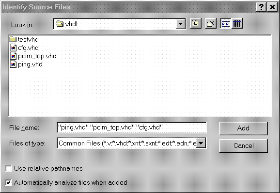 Figure 1- Read VHDL files into project 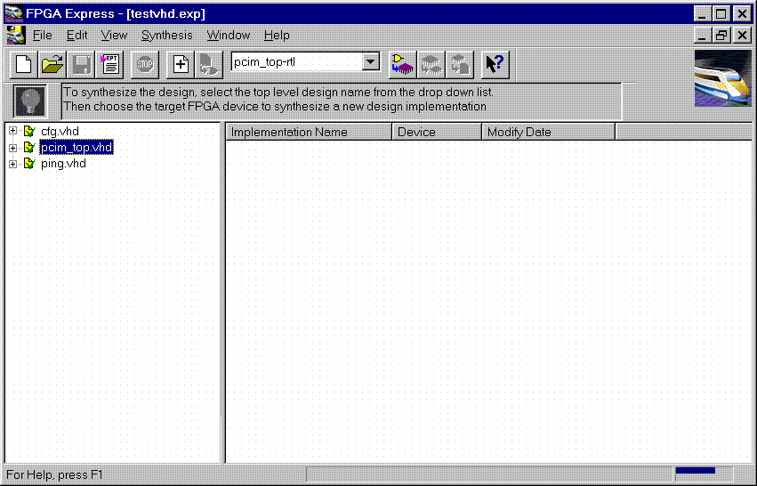 Figure 2- VHDL files analyzed (4) After the files have been 'analyzed', create an implementation. When the 'Create Implementation' window appears, set 'Family' to XC4000; set 'Device' to 4013xlpq208; set 'Speed grade' to -1. Check the box 'Do not insert I/O Pads'. 4013xlhq240-1 is also a valid part type for the PCI LogiCORE v2.0. (The PCI LogiCORE can also be used with the 4062xlpq208-1 or 4062xlhq240-1) 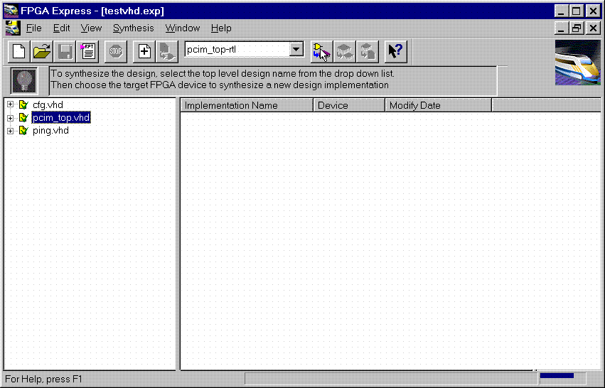 Figure 3- Implement the Design 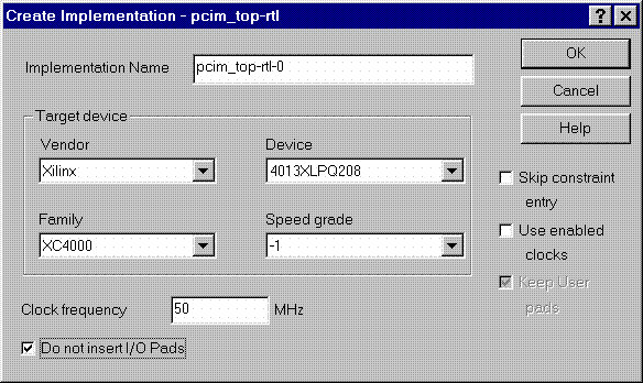 Figure 4- Create Implementation Window By default, FPGA Express v1.2 automatically inserts the correct I/O cells. The PCI LogiCORE v2.0 already has I/O inside of it. FPGA Express v1.2. can only insert all I/O cells or none at all. If FPGA Express was allowed to behave in its 'default' way, a syntactically incorrect netlist would be created. FPGA Express must be prevented for inserting I/O cells. I/O cells for the user application, in this case 'ping', must have the I/O cells instantiated manually. (5) Double-click on the implemenation that was created. A 5-tab window will appear. Select the 'Modules' tab. 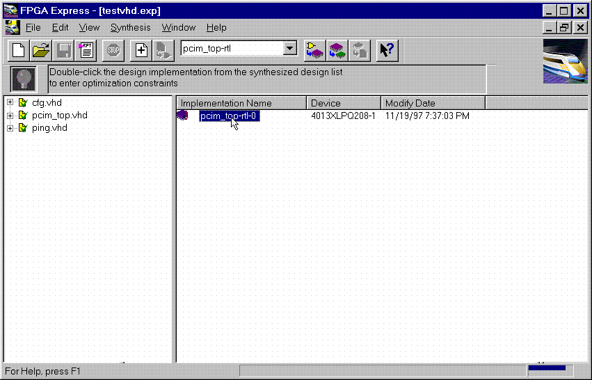 Figure 5- Open implementation 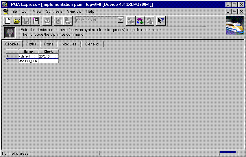 Figure 6- Implementation View (6) Under Modules, four items will be listed: IBUF, PCI_CORE, OBUF, and PING. Place a 'preserve' on all four items. 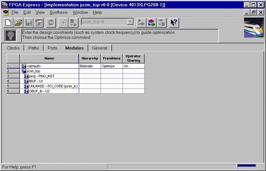 Figure 7- Implementation-Modules view For a user design, a preserve must always be placed on PCI_CORE, any instantiated I/O, and on the user application (in this case ping).  Figure 8- 'Preserve' attribute applied (7) Apply constraints in the implementation window as desired. Constraints can be applied via the 'Clock', 'Path', & 'Ports' tabs in the implementation window. (8) Close the implementation and 'optimize'(synthesize) the design. 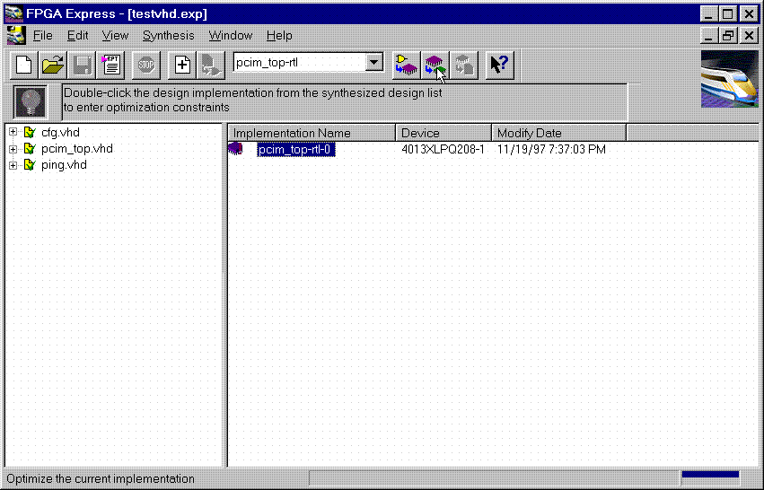 Figure 9- Optimize (9) If optimization is succesful, write out the XNF files for the design. Place the XNF files in the c:\mypci directory. Two XNF files will be produced by FPGA Express. One file will be named after the top-level design file (in this case pcim_top.xnf). The other file will be named after the user application (in this case ping.xnf). (10) Copy the following files into the c:\mypci directory: copy c:\pcim\vhdl\src\xpci\pcim_lc.sxnf c:\mypci\pcim_lc.xnf copy c:\pcim\vhdl\src\xpci\pci_lc_i.ngo c:\mypci copy c:\pcim\vhdl\src\ucf\m13xp208.ucf c:\mypci copy c:\pcim\vhdl\src\guide\m13xp208.ncd c:\mypci pcim_lc.sxnf must always be used. Be sure to re-name it to the extension .xnf. This file merges the core with the design correctly and contains needed constraints. pci_lc_i.ngo is the PCI LogiCORE v2.0 design. A constraint file included with the PCI LogiCORE v2.0 must be used. There are four constraint files in the cpcim\verilog\src\ucf directory. There are two UCF files for the 4013XLT. There are two UCF files for the 4062XLT. The 4013xlpq208 guide file was used in this example. (11) Place and route the design by running the following commands in the c:\mypci directory. Optionally, the listed commands below can be placed in a batch file: set XIL_MAP_LOC_CLOSED=true ngdbuild -p 4013xlpq208-1 -uc ../../src/ucf/s13xp208_1.ucf pcim_top.xnf map -pr o pcim_top.ngd -o pcim_top.ncd pcim_top.pcf par -gm exact -gf ../../src/guide/m13xp208 -d 1 -w pcim_top pcim_top_routed pcim_top trce -v 10 pcim_top_routed pcim_top ngdanno pcim_top_routed ngd2ver -w pcim_top_routed Solution 2: Timing Simulation with the PCI LogiCORE v2.0 and M1.3.7. (1) After place and route, a structural VHDL file, pcim_top_routed.vhd, and an SDF file, pcim_top_routed.sdf, will be in the c:\mypci directory. (2) Setup your Verilog simulator to use the M1.3.7 Verilog simulation libraries, which are located in %XILINX%\dl\src. (3) Simulate the PCI LogiCORE design, by reading in the pcim_top_routed.vhd file, pcim_top_routed.sdf file, and testbench file into the VHDL simulator. In this case for the ping design, the 'testbench' is comprised of the following files: c:\pcim\vhdl\example\source\ping_tb.v c:\pcim\vhdl\example\source\stimulus.v c:\pcim\vhdl\example\source\dumb_target.v c:\pcim\vhdl\example\source\dumb_arbiter.v Solution 3: Functional simulation with the PCI LogiCORE v2.0 and M1.3.7. (1) Get a list of files needed to functionally simulate the PCI LogiCORE. At the root directory of your system, type: cd c:\pcim\vhdl\example\func_sim (2) The func_sim direcory will contain a file called analyze_ping, which lists the files needed for functional simulation. The default list of files are located relative to the func_sim directory. The files needed for functional simulation are: ..\..\src\xpci\pci_lc_i.vhd -Simulation model for the PCI LogiCORE v2.0 ..\..\src\xpci\pcim_lc.vhd -Simulation model for the PCI LogiCORE v2.0 ..\source\cfg.vhd -Used for configuration of PCI LogiCORE v2.0 ..\source\ping.vhd -User application ..\source\pcim_top.vhd -Top-level file which connnects core to ping ..\source\dumb_target.vhd -signal generation for testbench ..\source\dumb_arbiter.vhd -signal generation for testbench ..\source\stimulus.vhd -signal generation for testbench ..\source\ping_tb.vhd -testbench For a user design, the ping.vhd file is replaced with the user VHDL code. At a minimum cfg.vhd, pcim_lc.vhd, and pci_lc_i.vhd must always be used. (3) Setup your VHDL simulator to use to the VITAL simulation library in M1.3.7. The VITAL simulation library is located at %XILINX%\vhdl\src (4) Functionally simulate the PCI LogiCORE v2.0 by processing the list of files in step (2) into the VHDL simulator. End of Record #3108 - Last Modified: 10/01/99 14:41 |
| For the latest news, design tips, and patch information on the Xilinx design environment, check out the Technical Tips! |