

|
|
| |
|
Answers Database
LogiCORE PCI32 4000: Verilog synthesis/simulation with PCI LogiCORE v2.0, FPGA Express v2.0.2, & M1.4.12
Record #3267
Product Family: Software ../source/ping_tb.v -testbench file ../source/stimulus.v -signal generation used in testbench ../source/dumb_target.v -signal generation used in testbench ../source/dumb_arbiter.v -signal generation used in testbench ../source/pcim_top.v -top-level Verilog file which connects core to ping ../source/ping.v -ping design(user applications) ../source/cfg.v -Used to configure features in the PCI LogiCORE v2.0 ../../src/xpci/pcim_lc.v -Verilog simulation model of the PCI LogiCORE v2.0../../src/xpci/pci_lc_i.v -Verilog simulation model of the PCI LogiCORE v2.0 For a user design, the ping.v file is replaced with the user Verilog code. At a minimum cfg.v, pcim_lc.v, and pci_lc_i.v must always be used. (3) Setup your Verilog simulator to point to the Verilog simulation library in M1.4.12. The Verilog simulation library is located at %XILINX%\verilog\data. (4) Functionally simulate the PCI LogiCORE v2.0 by processing the list of files in step (2) into the Verilog simulator. Solution 2: Synthesis/Place & Route of the PCI LogiCORE v2.0 with FPGA Express v2.0.2 and M1.4.12 (1) Assuming that 'pcim' is installed in your root directory, copy the following Verilog files into a directory of your choice. For this example, the directory is c:\mypci: copy c:\pcim\verilog\example\source\ping.v c:\mypci copy c:\pcim\verilog\example\source\cfg.v c:\mymci copy c:\pcim\verilog\example\source\pcim_top.v c:\mypci (2) Start FPGA Express and create a project in c:\mypci. (3) After creating the project, read in the files in the mypci directory into the FPGA Express project. 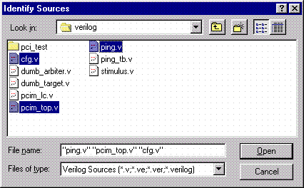 Figure 1- Read Verilog file into project 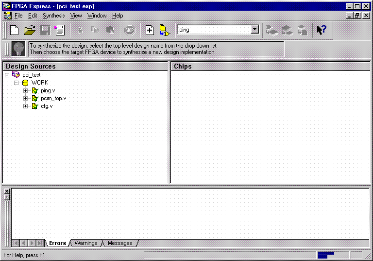 Figure 2- Verilog files analyzed (4) After the files have been 'analyzed', create an implementation. When the 'Create Implementation' window appears, set 'Family' to XC4000; set 'Device' to 4013xlpq208; set 'Speed grade' to -1. Check the box 'Do not insert I/O Pads'. 4013xlhq240-1 is also a valid part type for the PCI LogiCORE v2.0. (The PCI LogiCORE can also be used with the 4062xlpq208-1 or 4062xlhq240-1) 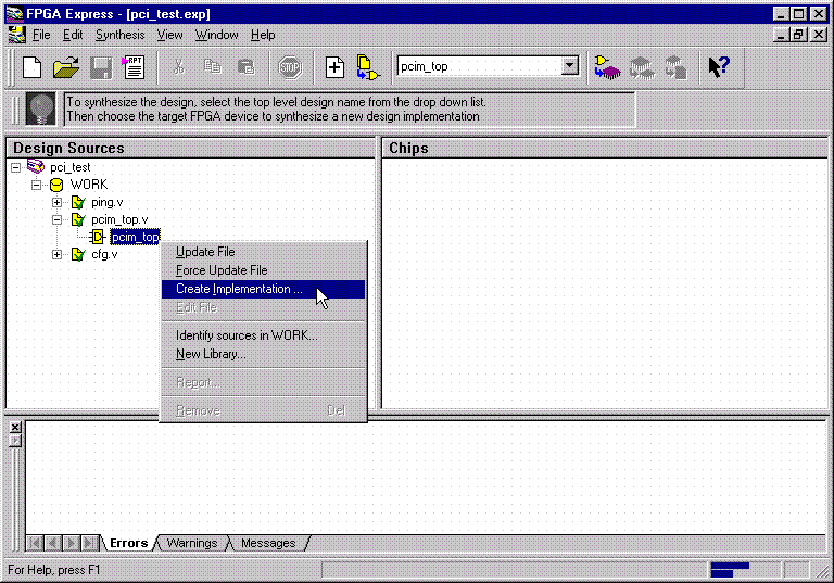 Figure 3- Implement the Design 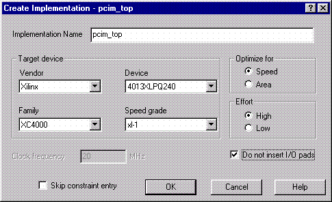 Figure 4- Create Implementation Window By default, FPGA Express v2.0.2 automatically inserts the correct I/O cells. The PCI LogiCORE v2.0 already has I/O inside of it. FPGA Express v2.0.2 can only insert all the I/O cells or none at all. If FPGA Express was allowed to behave in its 'default' way, a syntactically incorrect netlist would be created. FPGA Express must be prevented for inserting I/O cells. I/O cells for the user application, in this case 'ping', must have the I/O cells instantiated manually. (5) Right click on the new implementation of pcim_top and select Edit Constraints. Under the Modules tab, set the instantiated modules to "Preserve", as shown in Figure 5. 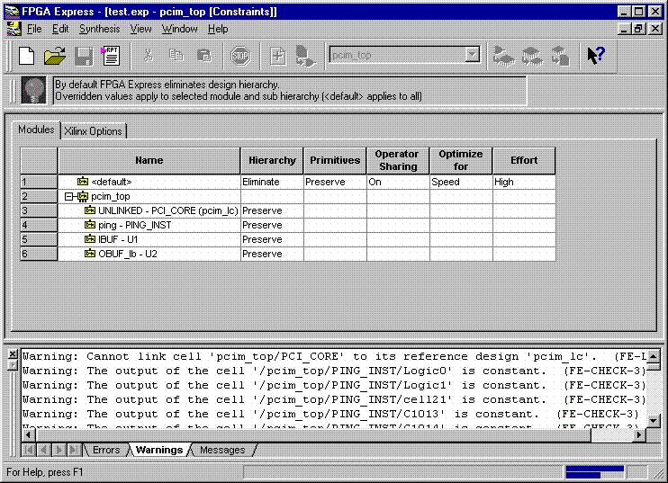 Figure 5- Preserve Hierarchy (6) 'optimize' (synthesize) the design. 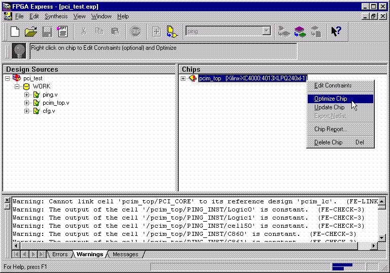 Figure 6- Optimize (7) If optimization is succesful, write out the XNF files for the design. Place the XNF files in the c:\mypci directory. Two XNF files will be produced by FPGA Express. One file will be named after the top-level design file (in this case pcim_top.xnf). The other file will be named after the user application (in this case ping.xnf). (8) Copy the following files into the c:\mypci directory: copy c:\pcim\verilog\src\xpci\pcim_lc.sxnf c:\mypci\pcim_lc.xnf copy c:\pcim\verilog\src\xpci\pci_lc_i.ngo c:\mypci copy c:\pcim\verilog\src\ucf\m13xp208.ucf c:\mypci copy c:\pcim\verilog\src\guide\m13xp208.ncd c:\mypci pcim_lc.xnf must always be used. This file merges the core with the design correctly and contains needed constraints. pci_lc_i.ngo is the PCI LogiCORE v2.0 design. A constraint file included with the PCI LogiCORE v2.0 must be used. There are four constraint files in the c:\pcim\verilog\src\ucf directory. There are two UCF files for the 4013XLT, one for the 4028XLT, and three for the 4062XLT. The 4013xltpq208 guide file was used in this example. (9) Place and route the design by running the following commands in the c:\mypci directory. Optionally, the listed commands below can be placed in a batch file: set XIL_MAP_LOC_CLOSED=true ngdbuild -p 4013xlpq208-1 -uc c:\mypci\s13xp208_1.ucf pcim_top.xnf map pcim_top.ngd -o pcim_top.ncd pcim_top.pcf par -gm exact -gf c:\mypci\m13xp208 -l 4 -d 1 -w pcim_top pcim_top_routed pcim_top trce -v 10 pcim_top_routed pcim_top ngdanno pcim_top_routed ngd2ver -w pcim_top_routed Solution 3: Timing Simulation with the PCI LogiCORE v2.0 and M1.4.12. (1) After place and route, a structural Verilog file, pcim_top_routed.v, and an SDF file, pcim_top_routed.sdf, will be in the c:\mypci directory. (2) Setup your Verilog simulator to use the M1.4.12 Verilog simulation libraries, which are located in %XILINX%\verilog\data. (3) Simulate the PCI LogiCORE design, by reading in the pcim_top_routed.v file, pcim_top_routed.sdf file, and testbench file into the Verilog simulator. In this case for the ping design, the 'testbench' is comprised of the following files: c:\pcim\verilog\example\source\ping_tb.v c:\pcim\verilog\example\source\stimulus.v c:\pcim\verilog\example\source\dumb_target.v c:\pcim\verilog\example\source\dumb_arbiter.v End of Record #3267 - Last Modified: 10/01/99 14:40 |
| For the latest news, design tips, and patch information on the Xilinx design environment, check out the Technical Tips! |