Answers Database
LogiCORE PCI: Inserting initial latency in a target design

Record #7300
Product Family: Documentation
Product Line: LogiCore
Product Part: PCI Master Release Notes
Product Version: 2.0
Problem Title:
LogiCORE PCI: Inserting initial latency in a target design
Problem Description:
Urgency: Standard
General Description:
What is the methodology for inserting wait states in a target transaction?
Solution 1:
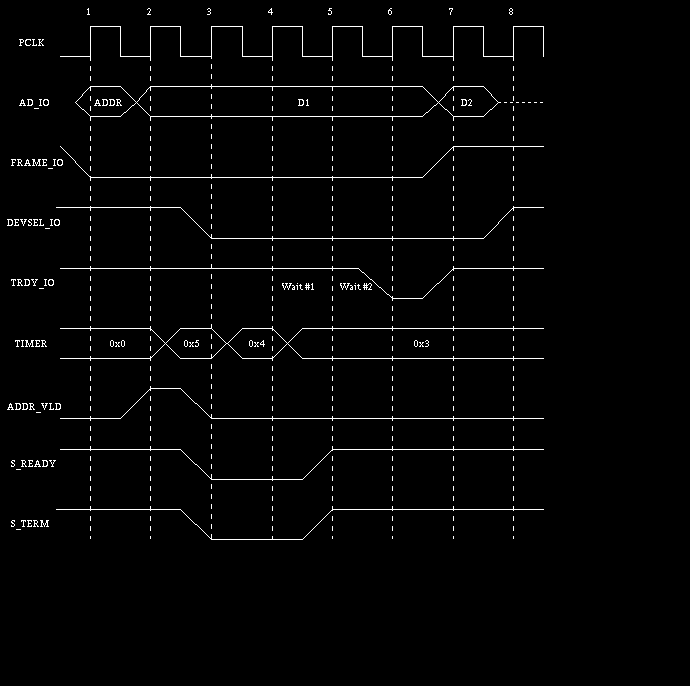
In Chapter 6 of LogiCORE PCI Design Guide ("Target Data Phase Control"),
Example 3 talks about initial latency, and how to insert initial wait states.
This Answer will address exactly how to read the pseudo code.
On clock cycle 1, the Address is valid on AD_IO (the external PCI bus) and
FRAME_IO has been asserted. For clarity, we are assuming that a Reset
just took place, so the value of TIMER is 0.
On clock cycle 2, the first DWORD is presented on AD_IO, and
ADDR_VLD is asserted to the user application. Not shown in the
waveforms below, ADDR is valid to the user application as well. Since
ADDR_VLD is asserted, TIMER is set to whatever BL_WAIT is.
BL_WAIT = number of wait states to be inserted + 3. During clock 2,
S_READY and S_TERM are set to 0, since the boolean compare
(TIMER <= 4'h3) is now false.
On clock cycle 3, BASE_HIT[x] would be asserted, signaling the
transaction is targeting the Xilinx PCI device. At this point, S_READY
and S_TERM are checked, and TRDY_IO would be asserted on the
following clock if S_READY = 1. The Xilinx LogiCORE provides a
medium decode for addresses, so DEVSEL_IO is asserted in time for
the rising edge of clock 3. Since S_READY and S_TERM are both
deasserted, a wait state will be inserted on clock 4. TIMER is
decremented to 4.
On clock cycle 4, S_READY and S_TERM are checked to determine the
state of TRDY_IO on clock 5. S_READY and S_TERM are still
deasserted, so another wait state will be asserted on clock 5. TIMER is
decremented to 3 on the clock edge, so S_READY and S_TERM are
asserted combinatorially during clock 4, signaling a Disconnect with Data.
The second (and final) wait state is inserted. S_READY and S_TERM are
sampled on the rising edge of clock 5, signaling a Disconnect with Data
on clock 6. TRDY_IO is asserted and STOP_IO is asserted during clock 5
due to this.
The data is transferred on the rising edge of clock 6. By the PCI spec,
STOP_IO is required to remain asserted, and TRDY_IO is deasserted
during clock 6. Since FRAME_IO (and DEVSEL_IO) are still asserted,
the initiator places another DWORD on the PCI bus. Since STOP is
asserted on the rising edge of clock 6, FRAME_IO is deasserted during
clock 6.
Since STOP_IO is asserted and TRDY_IO is deasserted on the rising
edge of clock 7, DEVSEL_IO is deasserted, ending the transaction.
D2 is never transferred.
Insertion of Wait States in a Target Write
End of Record #7300 - Last Modified: 08/23/99 17:22 |

