|
||
Home : Products : Devices : Virtex-II Platform FPGAs
|
||||||||||||||||||||||
|
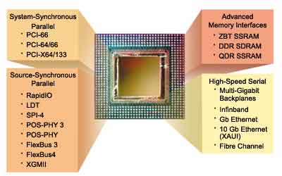
Welcome To The Era Of The Platform FPGA It's an era where Xilinx leads the way, strengthened by our strategic alliances with IBM, Wind River Systems, Conexant, RocketChips, The MathWorks, and other technology leaders. The Platform FPGA delivers SystemIO™ interfaces to bridge emerging standards, XtremeDSP™ for unprecedented DSP performance (up to 100 times faster than the leading DSP processor), and will offer Empower!™ processor technology for flexible high-performance system processing needs. The Virtex-II solution is the first embodiment of the Platform FPGA, once again setting a new benchmark in performance, and offering a feature set that is unparalleled in the industry. The Ultimate System Design Platform With densities ranging from 40,000 up to 10 million system gates, the Virtex-II solution delivers enhanced system memory and lightning -fast DSP through a flexible IP-Immersion fabric. Additionally, significant new capabilities address system-level design issues including flexible system interfaces with signal integrity (SystemIO™ , XCITE™ ), complex system clock management (Digital Clock Manager), and on-board EMI management (EMIControl™ ). Virtex-II solutions are empowered by advanced design tools that drive time to market advantages through fast design, powerful synthesis, smart implementation algorithms, and efficient verification capabilities. Not only does the fabric provide the ability to integrate a variety of soft IP, but it also has the capability of embedding hard IP cores such as processors and Gigabit serial I/Os in future Virtex-II families. SystemIO™ —The Premier System Connectivity Solution SystemIO™ fully addresses all aspects of system connectivity in high-performance designs. System connectivity consists of the physical interface and the protocols required to offer higher bandwidth. The Virtex-II SystemIO technology uses the SelectI/O-Ultra™ blocks to provide the fastest and most flexible electrical interfaces available. Each user I/O pin is individually programmable for any of the 19 single-ended I/O standards or six differential I/O standards, including LVDS, SSTL, HSTL II, and GTL+. SelectI/O-Ultra technology delivers 840 Mbps LVDS performance using dedicated Double Data Rate (DDR) registers. IP for RapidIO, POS PHY 4, Flexbus 4, LDT and other source-synchronous bus standards are available through Xilinx. Popular PCI-66 and PCI-X 133MHz IP is also easily accessible from our IP Center. Designers can now pick and choose the necessary interfaces customized for their applications. Furthermore, any two I/O pins can be used as a differential pair, providing maximum board lay-out flexibility. Multi-gigabit serial interfaces will be incorporated in future Virtex-II families based on Conexant’s Skyrail™ and RocketChips’™ technologies.
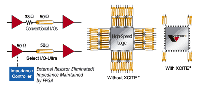
XCITE™—The Industry’s First Digitally Controlled Impedance Technology The Xilinx® Controlled Impedance Technology (XCITE) in the Virtex-II solution dynamically eliminates drive strength variation due to process, temperature, and voltage fluctuation. XCITE uses two external high-precision resistors to incorporate equivalent input and output impedance internally for hundreds of I/O pins. As systems get faster, high signal integrity is critical to ensure maximum performance. The XCITE option is available when users select the I/Os to be any of the 19 single-ended standards. This reduces on-board resistors, provides significant system cost reduction and reduces board re-spins. The XCITE technology reduces board layout complexity while increasing reliability.
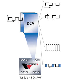
The Perfect Choice For High-Speed Clock Design Twelve 400+MHz Digital Clock Managers: Virtex-II devices contain up to 12 Digital Clock Managers (DCMs) Each DCM provides phase shifting and frequency synthesis capabilities, which are ideally suited for systems with multiple clock domains and critical timing requirements. The DCM delivers unsurpassed flexibility for managing both on-chip and off-chip clock synchronization. Virtex-II DCMs support 400+MHz clock outputs to enable leading-edge bus interface standards such as RapidIO and SPI-4. The digital nature of the DCM makes it impervious to system temperature and voltage variations. The benefits of the DCM include: Digital Clock Manager
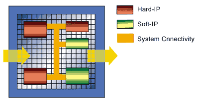
Sixteen Pre-Engineered Clock Domains: Each Virtex-II device has 16 pre-engineered clock domains to support the multiple frequency and multiple phase requirements of complex system designs. Each built-in, low-skew clock network eliminates complex clock tree analysis and simplifies the system design process. EMIControl™ —A First In Programmable Logic The Virtex-II solution is the first programmable family to provide innovative spread spectrum clocking technology to reduce Electro Magnetic Interference (EMI) noise emissions. Digital spread spectrum (DSS) technology broadens the output clock frequency spectrum to reduce EMI and meet FCC regulations. This feature allows the designer to greatly reduce system cost and design cycles by minimizing board re-spins and eliminating expensive shielding. IP-Immersion™ Architecture The Virtex-II IP-Immersion architecture enables easy integration of on-chip hard-IP blocks and a broad library of soft-IP blocks. Complex IP-based designs can incorporate an abundance of advanced routing resources, on-chip memories, and embedded multipliers.
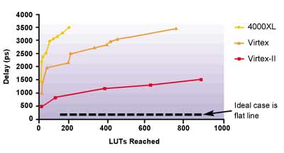
Active Interconnect™ Technology The Active Interconnect™ technology is developed specifically for the high-performance wide system bus needs of today’s complex designs. Multi-million gate designs very often have many high fan-out nets which are optimally accommodated by the abundant and fully active routing resources of the Active Interconnect technology. Furthermore, Active Interconnect technology plays a critical role in IP portability and reuse by providing consistent and predictable high-performance.
Highest Memory to Logic Ratio The high density on-chip memory in the Virtex-II solution increases overall system bandwidth by providing fast and resource efficient FIFO buffers, shift registers, and CAM. The enhanced SelectRAM+™ hierarchy of the IP-Immersion architecture, consisting of distributed RAM, block RAM, and high-speed memory interfaces, provides a powerful memory-based data-path fabric for bandwidth intensive systems. The Virtex-II solution provides industry’s highest memory to logic ratio with up to 3.5Mb of on-chip block RAM and delivers over 400Mbps DDR/QDR memory interface performance.
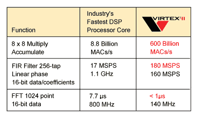
XtremeDSP Performance With embedded multipliers and improved arithmetic functions, the Virtex-II solution delivers over 600 Billion MACs/s of XtremeDSP performance. There are up to 192 18 x 18 multipliers in a single device, supporting up to 18-bit signed or up to 17-bit unsigned representation, and cascading to support bigger numbers. The multipliers can be fully combinatorial running between 140 and 250 MHz depending on bit width. Designers can use Virtex-II devices to implement critical DSP elements of emerging broadband systems such as sub-1-microsecond 1024 point FFTs, ultra-fast adaptive filters, 3G turbo coder, rake receivers, and spread spectrum.
A New Level Of Design Security The Virtex-II solution provides design security through bitstream encryption. The bitstream is encrypted using a secure triple Data Encryption Standard (DES) algorithm. The key is supplied through the IEEE 1149.1 JTAG interface, which is stored inside the chip using either a battery or other constant power supply. The encrypted bitstream is loaded into the FPGA with specific key bank designated for decryption. This feature provides high design security to prevent design theft, and enables an entirely new business model for IP providers.
Advanced Design Methodology The Virtex-II FPGA is accompanied by a suite of sophisticated design tools that support the industry’s fastest runtimes and the most advanced design methodologies. The innovative incremental design flow facilitates efficient ‘what if’ analysis, accelerates timing closure, and increases system performance. High-level floorplanning and modular design make it easy to realize the promise of true team design. Xilinx System Generator™ together with The MathWorks’ MATLAB and Simulink provide a powerful design package using tools that are familiar to system and DSP designers. These design tools and the library of Xilinx SmartIP enable designers to increase overall productivity and reduce the design cycle.
Xilinx Development Systems speed your time to market. Solving The Verification Bottleneck The programmability of the Virtex-II FPGA ensures that many time consuming verification tasks such as chip-level signal integrity analysis and scan insertion are unnecessary. Xilinx design tools provide complete support for all verification checkpoints including RTL Simulation, accelerated timing simulation, and even powerful static timing analysis. Board-level verification is supported through STAMP and LMG Smart models. ChipScope ILA from Xilinx provides real-time, on-chip de-bugging, in conjunction industry leading logic analyzers. Wide busses, complex triggering and multiple clocks are easily managed using ChipScope ILA cutting de-bugging time from weeks to just a few hours. |
|||||||||||||||||||||
|
| Home | Products | Support | |