|
|
The Industry's First General-Purpose 64-bit, 66 MHz PCI Solution now supports Virtex-II
|
|

|
|
The Virtex, Virtex-E and Virtex-II FPGA families meet demand for compliance, flexibility, and performance with 66 MHz PCI -- before the availability of standard chips, ASICs and specialized FPGAs.
LogiCORE PCI 64/66 product for Virtex, Virtex-E and Virtex-II FPGAs
|
|
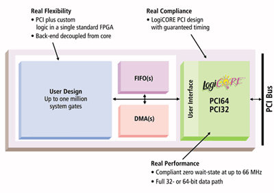
The Real PCI from Xilinx enables designers to implement a 64-bit, 66 MHz PCI interface in a standard Virtex, Virtex-E, Virtex-II FPGA, for communications storage and video imaging applications.
- Fully PCI specification V2.2 compliant interface supporting a sustained throughput of 528 Mbytes/second.
- Decoupled back-end design allowing user to add dual-port customized FIFOs, DMA controller, and other custom logic functions.
|

|
|
|
|

|
| Key Features |
|
Real Availability - Cores and the devices are available today
Real Compliance - Timing is guaranteed by Smart-IP technology |
Real Flexibility - Targeted to Xilinx standard Virtex familiy FPGAs
Real Performance - Zero wait-state burst and 64-bit back-end interface |
|
Real Availability
The 64/66 PCI LogiCORE design is available for Virtex, Virtex-E and Virtex-II devices. All Virtex and several Virtex-E devices are available today. See datasheet for specific devices and packages.
Since September 1998, more than a dozen beta customers have already been using
the Real 64/66 PCI in applications such as Gigabit Ethernet, ATM and Fiber Channel
adapters, DSP/Imaging boards, disk drive arrays and high-end printer interfaces.
Beta customers include Ascend Communications, Dome Imaging, and Kodak.
|
|
The Dome Imaging MX2/PCI board is the first in a new family
of high resolution display controllers for the medical imaging market that can handle
transfers of over 500 MB/s from the host.
|
"With the Real 64/66 PCI products from Xilinx, we were able to implement
a fully compliant PCI interface - plus other functions such as direct memory access
(DMA), 4 dual-port FIFOs, and 200,000 gates of our own unique design - in a single
device," said John Beck, Principal Engineer from DOME Imaging, Inc. "After
evaluating different solutions in the market, we found that only Xilinx could meet
the demanding requirements for full 66 MHz PCI compliance." |
Real Compliance
The Real 64/66 PCI solution provides full protocol,
timing and electrical PCI v2.2 compliance. Thanks to the fast multi-standard
SelectI/OTM interfaces
in a Virtex FPGA, a single I/O buffer per PCI signal can be used, which is required
to meet the PCI specification.
The Real 64/66 PCI core is based on the already proven 32-bit PCI solution from
Xilinx that to date has been used in more than 1,000 customer designs. It is verified
with Xilinx internal testbench that simulates over 6 million PCI cycles, which ensures
a high-quality PCI product.
To minimize customers' development time, The Real 64/66 PCI core guarantees all
the critical PCI timing. We achieve this by characterizing the Virtex silicon together
with the LogiCORE PCI design and then applying strict implementation constraints.
As a result, the implementation of the most critical parts of the PCI core looks
exactly the same every time the core is compiled, independent of the tools that are
used and independent of the customers' unique back-end design. We call this method
of guaranteeing the timing with maintained flexibility Smart-IP technology and it
is only available from Xilinx.
The guarantee includes the extremely challenging 3ns maximum setup time, 2ns minimum
clock-to-out, and 0ns hold time of the Critical Path shown in the figure below. The
Critical Path becomes the constraint when decoding the Initiator Ready (IRDY) and
Target Ready (TRDY) signals, which must be completed at full speed in an Initiator
interface bursting data without wait-states.
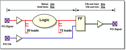
The Critical Path
|
Real Flexibility
The Real 64/66 PCI from Xilinx is a firm core targeted to our standard off-the-shelf
Virtex and Virtex-E FPGA families. Because the PCI interface is implemented in a
standard FPGA and not a specialized FPGA with an embedded PCI interface, you will
benefit from unparalleled flexibility, still with guaranteed 66MHz PCI timing.
There are several benefits of this methodology
- You do not have to qualify a separate component for your PCI design
- You can select between several device sizes and packages
- You will benefit from the large-scale manufacturing of standard FPGAs, which
results in the lowest possible cost and highest performance
- You can adapt to future changes of the PCI specification, and future design requirements.
As you know, PCI is a moving target and it is very difficult to anticipate future
requirements
PCI Design Files Over the Internet
|
|
As part of Xilinx Silicon Xpresso initiative, all LogiCORE PCI design files are
distributed over the Internet and are available in the Xilinx PCI Lounge, a password
protected area on this website.
LogiCORE PCI V3.0, Configuration
and Download (Demo Version)
The download procedure couldn't be simpler:
- Configure the core in the intuitive, menu driven graphical user interface
- Click on download, and the tool will generate an EDIF netlist, simulation models
and instantiation code in VHDL and Verilog, and all the implementation constraints
required to guarantee the timing of the core design.
|
 |
| The PCI design is Supported with the Following Design Tools |
|
Design Entry:
- Synopys FPGA Compiler and FPGA Express
- Synplicity Synplify
- Exemplar Leonardo Spectrum
|
Design Verification:
- Cadence Verilog XL
- Model Technology ModelSim
- Aldec Active VHDL
|
|
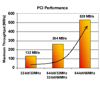
Real Performance
The Real 64/66 PCI from Xilinx offers up to the maximum sustained throughput of
528 Mbytes per second. This is achieved by:
- A true 64-bit data path throughout the core
- Zero wait-state burst capability
- On-chip dual-port FIFOs that can be scaled to fit your system requirements.
|
|
|
PCI Training
To further complete the Xilinx PCI solution, Xilinx offers two PCI classes for customers who are planning PCI systems. The one day PCI Basics class will give an introduction
to the PCI standard and Xilinx PCI solution. The two day class on Designing a PCI System will cover configuration and integration of the core, PCI system design and verification.
XPERTS Design Services
To support your PCI design you have worldwide access to certified PCI
experts that can provide design services including:
- Support for targeting additional devices
- Implementation of additional features
- Complete turnkey integration
More Information
 to view the to view the  PDF
files below PDF
files below
|
|