|
||
|
| ||
| techXclusives | ||||
|
| ||||
|
||||
|
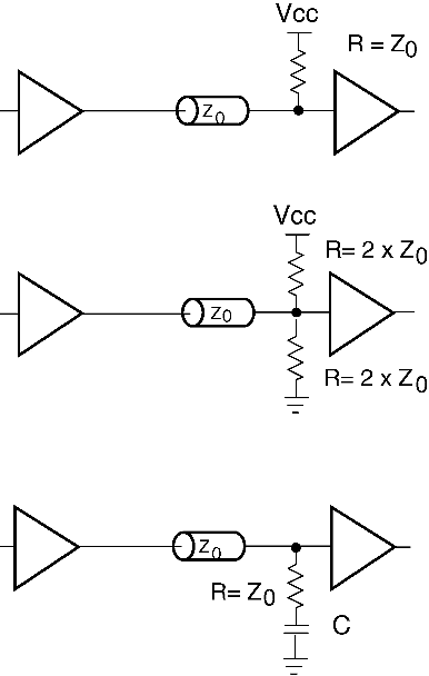
Layout Considerations The PC board is no longer just a means to hold ICs in place. At today's high clock rates and fast signal transitions, the PC board performs a vital function in feeding stable supply voltages to the IC and in maintaining signal integrity between devices. VCC and Ground Planes Since CMOS power consumption is dynamic, it is a non-trivial task to assure stable supply voltages at the device pins and to minimize ground differentials. A multi-layer PC board is a must, with four layers for the simplest circuits, 6 to 12 layers for typical boards. Ground and VCC must each be distributed in complete layers with few holes. Slots in these layers would cause an unacceptable inductive voltage drop when the supply current changes at a rate of 1 A/ns, or even faster. Besides an uninterrupted ground plane, Virtex-II devices require one plane for VCCINT (1.5V), plus one plane for VCCAUX (3.3V). VCCO can be distributed on wide signal traces with sufficient bypass capacitors. Beyond low resistance and inductance, ground and VCC planes combined can also provide a small degree of VCC decoupling. The capacitance between two planes is ~100 pF/inch2 or -15 pF/cm2, assuming 10 mil (0.25 mm) spacing with FR4 epoxy. VCC Decoupling Fast-changing ICC transitions must be supplied by local decoupling capacitors, placed very closely to the VCC device pins or balls. These capacitors must have sufficient capacitance to supply ICC for a few ns, and must have low intrinsic resistance and inductance. X7R or NPO ceramic surface-mounted capacitors of 0.01 to 0.1 uF can supply 1A for 2ns with a 20 m V voltage droop. 1A * 2ns = 2 nanocoulomb = 100 nF * 0.02 V Low impedance at >100 MHz is important, but capacitance variation with temperature is acceptable. These small capacitors are the first-line source for ICC, and they must be placed very close to the VCC pins. A half-inch or 10 mm trace represents an inductance of several nanohenries, defeating the purpose of the decoupling capacitor. Backing up this local decoupling is one tantalum capacitor of 10 to 100 uF, able to supply multiple amperes for about 100 ns. Finally, each board needs a power-supply decoupling electrolytic capacitor of 1000 to 10,000 uF able to supply even more current for a portion of the supply switching period. As described below, larger capacitors inevitably have a higher series resistance and inductance, which is the reason for the above-mentioned hierarchy of supply decoupling. As a general rule, multiple capacitors in parallel always offer lower resistance and inductance than any single capacitor. Transmission Line Reflections and Terminations A PC board trace must be analyzed as a transmission line. Its series resistance and parallel conductance can generally be ignored, but series inductance and parallel capacitance per unit length are important parameters. Any signal transition (rising or falling edge) travels along the trace at a speed determined by the incremental inductance or capacitance. For an outer-layer trace (air on one side), the propagation delay is 140 ps/inch, or 55 ps/cm. For an inner-layer trace (FR4 with E = 4.5 on both sides), the propagation delay is 180 ps/inch, or 70 ps/cm. The voltage-to-current ratio at any point along the transmission line is called the characteristic impedance Z0. It is determined by w/d, the ratio of trace width "w" to the distance "d" above the ground or VCC plane. For an outer layer trace (microstrip): Z0=50 ohms when w = 2d (e.g., w = 4 mil, d = 2 mil), Z0=75 ohms when w = d (e.g., both 2 mil = 0.5mm). For an inner layer trace (stripline): Z0=50 ohms when w = 0.6*d (e.g., w = 4 mil, d = 2 mil), Z0=75 ohms when w = 0.25*d (impractical). Most signal traces fall into the range of 40 to 80 ohms. A slow transition treats a short narrow trace as a lumped capacitance of about 2pF per inch (0.8 pF per cm). However, if the trace is so long, or the signal transition is so fast that the potential echo from the far end arrives after the end of the transition, then the trace must be analyzed as a transmission line. In this case, the driver sees the trace not as a lumped capacitance, but rather as a pure resistance of Z0. The signal transition then travels along the trace at the speed mentioned above. At any trace-impedance discontinuity, all or part of the signal is reflected back to the origin. If the far end is resistively terminated with R=Z0, then there is no reflection. If, however, the end if open, or loaded with only a CMOS input, then the transition doubles its amplitude, and this new wave travels back to the driver, where it may be reflected again, resulting in the familiar ringing. Such ringing has a serious impact on signal integrity, reduces noise margins, and can lead to malfunction, especially if an asynchronous signal or a clock signal crosses the input threshold voltage unpredictably. Two alternate ways to avoid reflections and ensure signal integrity are parallel termination and series termination. Parallel Termination Reflections from the far end of the transmission line are avoided if the far end is loaded with a resistor equal to Z0. A popular variation uses two resistors, one to VCC, and one to ground, as the Thevenin equivalent of Z0. This reduces the load current for one signal level, while increasing it for the other. Parallel termination causes dc power consumption, which can be eliminated by inserting a capacitor between the terminating resistor and ground. The value of this capacitor is determined as follows: Signal transition time << RC << signal level duration For example, 50 ohms * 120 pF for a 2 ns transition every 20 ns:
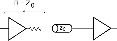
Series Termination While parallel termination eliminates reflections, series termination relies on the reflection from the far end to achieve a full-amplitude signal. For series termination, the driver impedance is adjusted to equal Z0, thus driving a half-amplitude signal onto the transmission line. At the unterminated far end, the reflection creates a full-amplitude signal, which then travels back to the driver where it gets absorbed, since the output impedance equals Z0.
Series termination dissipates no dc power, but the half-amplitude round-trip delay signal means that there must be no additional loads along the line. Series termination is ideal (and only meaningful) for single-source-single-destination interconnects. Virtex-II devices offer digitally controlled output impedance drivers and digitally-controlled input termination, thus eliminating the need for any external termination resistors. This feature is extremely valuable with high pin-count, high density packages. These PC board considerations apply to all moderns systems with fast current and voltage transitions, irrespective of the actual clock frequency. The designer of relatively slow systems is more likely caught off-guard by the inherent speed of modern CMOS ICs, where di/dt is measured in A/ns, dV/dt is measured in V/ns, and input flip-flops can react to 1 ns pulses that are invisible on mid-range oscilloscopes. Powerful tools like Hyperlynx can analyze signal integrity on the PC board and can often be amortized by one eliminated board-respin. Share your comments, questions and ideas with Peter Alfke and other interested designers at the "Printer Circuit Board Considerations" FORUM. |
||||