|
||
|
| ||
| techXclusives | ||||
|
| ||||
|
||||
IntroductionThere seems to be a lot more discussion lately about an old friend of mine: the variations in the significant instants of a clock or data signal. This is ITU-T definition of "jitter." Jitter is defined as those phase variations with respect to a perfect reference that happens in a clock or data signal as a result of noise, patterns, or other causes, with a frequency of variation greater than a few tens of Hertz. (Slower changes in phase due to temperature, voltage, and other physical changes are usually referred to as "wander." I will not discuss wander here, but rather concentrate on the causes, measurement, and management of jitter.) A more useful measure of jitter in a digital system is the "period" jitter. The period jitter is usually measured as the difference between the longest period and the shortest period. The period jitter is needed to ensure that there is adequate setup time for all of the signals. Causes of JitterA perfect oscillator would have rising edges occurring at precise moments in time that would never vary. This, of course, is impossible, as even the best rubidium, cesium, or hydrogen maser oscillators are constructed from real electronics, and have sources of noise and other imperfections. A high-quality, low-phase noise crystal oscillator will have a jitter of less than 35 picoseconds (ps) period jitter, accumulated over many millions of clock edges. This means that the maximum period vs. the minimum period of the oscillator will vary by no more than the peak-to-peak value. Lower jitter values are extremely difficult to achieve, so higher jitter values are quite common. Jitter is caused by thermal noise, instabilities in the oscillator electronics, external interference through the power, ground, and even through the output connections disturbing the oscillator. Oscillators are influenced by external magnetic or electric fields by contributing to jitter in their output. RF interference from nearby transmitters will also contribute to jitter. A simple amplifier, inverter, or buffer will add jitter to a signal. Poor signal integrity (SI) engineering that results in transmission line reflections, cross-coupling (cross talk), ground or Vcc bounce adds jitter to a signal; inadequate bypass or decoupling will also lead to increased jitter. Poor power supplies, and unstable Phase-Locked Loops (PLL's) are also common contributors to jitter in a system. Just about anything that can add noise to a signal or change the reference of an input buffer (such as ground bounce) will add jitter to the resulting signal. Measurement of Jitter Jitter represents the result of a statistical measurement process. As a consequence, the longer one measures jitter, the larger the measured value gets. At some point, the jitter stops increasing due to short-term variations, and the measurement continues to increase due to the physical changes that are always occurring. In order to make sensible measurements in a limited amount of time, instruments rely on either predicting the result by fitting a Gaussian distribution to the measurement, or by stating a confidence level. Millions of edges may have to be measured in order to be sure of the result. If the jitter is too large, it may lead to an error in the logic, which may have dire consequences. These problems may occur only once per day, and may be extremely difficult to find. Instrumentation has its own error, and in order to measure sub-nanosecond jitter, the instrument requires picosecond measurement resolution and accuracy.
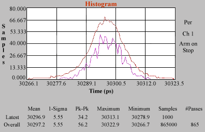
In this figure, the variations in every clock period sampled are plotted as a histogram of the number of periods with a given length. The outer curve is the accumulated count (in this case, 865,000 samples). The inner curve is the latest sampled count of 1000 periods. The peak-to-peak period jitter is noted as 34.2 ps for the latest block of 1000, and 56.2 Ps for the total of all samples. You could also state this as +/- 28.1 Ps of jitter (plus and minus peak). The 1-sigma (average) jitter is 5.55 Ps The minimum and maximum clock periods are also shown. (This data was taken from the Wavecrest DTS 2075 on a Virtex-300E using a Rhode & Swartz signal generator with an output jitter of ~25 Ps P-P under normal conditions.) Common types of jitter are: period jitter, cycle-to-cycle jitter, and ITU-T jitter. Period jitter is the stated as either the peak-to-peak, minimum and maximum, or average (RMS) (or some combination of these) of any and all periods measured. Cycle-to-cycle jitter is the peak-to-peak or average difference between adjacent cycles or periods. ITU-T jitter is defined as the worst case variation from any edge to a perfect mythical reference as peak-to-peak in unit intervals where one unit interval is equal to the clock period. ITU-T jitter may exceed the value of a single period by many times, as all of the edges may be running too fast or too slow, and the jitter will accumulate to a large value. For example, 10 UI (unit intervals) for a 10 ns clock period over 10,000 clocks is a 100 ns variation from any edge to a perfect reference. Period jitter is required for verifying that timing constraints have been met, cycle-to-cycle jitter is a variant on the period jitter, and ITU-T jitter is useful for predicting bit error rates on communications channels (wire, fiber, or radio). Jitter is commonly characterized, or measured, by its peak-to-peak value, minimum and maximum values, its RMS value or one sigma (a measure of its power, or energy), its frequency spectrum, and by other statistical measures useful for determining the causes of the jitter. Allen Variance or Time Deviation are commonly used to help identify causes due to the slope changes in the graphs for different physical causes of jitter. Management of JitterPhase-Locked Loops are commonly used to remove jitter. They may instead add their own intrinsic jitter or amplify the jitter if their loop gain and phase margin make them unstable. They may also be sources of jitter due to inadequate power supply rejection or coupling from other noise sources. A properly designed PLL can remove all objectionable jitter, and provide a high-quality clock signal. Long loop time constants are necessary; this results in increased wander for the benefit of decreased jitter. The basic rules of jitter management are: - Start with the highest quality clock signal. If an external clean-up PLL is required, perform the necessary Bode Plot stability analysis to be certain that you have a jitter attenuator, not a jitter amplifier. ConclusionIn the past, with clock rates slower than 100 MHz, 200 ps of total peak-to-peak jitter from all sources was not even considered as part of the design. With clock periods of 2.5 ns possible in Virtex-II, even the most careful design might accumulate 10% of the period as jitter (250 ps) when all I/O's are switching, all logic is operating on the device, and all DLLs are in use. Now that 10% of the period is lost to jitter, timing constraints must evaluate the critical path for constraints both 5% shorter and 5% longer than intended to verify the setup times of the design. Verification of jitter tolerance also has to be performed to insure that the design is robust enough to operate with all of the expected variations in components, temperatures, and voltages. In order to verify the timing margin, jitter should be added to the clock input until the design fails. You then can check to see that the margin is adequate or meets the system's specification. Added jitter should be through a sine wave modulation source, and swept over the range of ~100 Hz to the clock frequency divided by 1000. Higher rates of jitter modulation may also be necessary as well. For the jitter modulation frequency from the clock frequency divided by 1000 to the clock divided by 2, is also a range of possible test conditions for a SPI POS 4 design. Jitter is the next challenge to systems designers now in the high-speed, ultra- deep, sub-micron world. Reference textbooks: "Jitter in Digital Transmission Systems" "Digital Transmission Design and Jitter Analysis" Equipment suppliers to check out are: Wavecrest A good resource on time and frequency is: http://www.boulder.nist.gov/blconf.htm |
||||