|
||
|
| ||
|
|
||||||||
| techXclusives | ||||||||
|
| ||||||||
|
||||||||
|
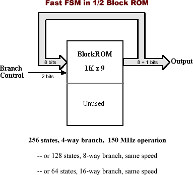
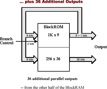
Virtex™-II offers many multipliers and block RAMs, four each in the smallest XC2V40, and forty in the middle-of-the road XC2V1000, even more at the high end. As many, if not most designs will not require exactly all these functional blocks, it is thus of interest to explore alternate uses for leftover multipliers and block RAMs in a design. Use the Multiplier as a ShifterA multiplier can be used as a shifter. One operand is routed to the output, shifted by n positions, if the other operand is a power of two (2n). Since the sign-bit (MSB) cannot be used to control the shift, the 18x18 2s-complement multiplier can shift by 0 to 16 positions. Of the 36 output lines, those less significant than the shifted data lines are automatically filled with zeros; those more significant than the shifted data are filled with zeros or ones, depending on the state of the MSB input. This is the natural result of the 2s-complement multiplication. The user can either perform a logic shift of 17 input bits by holding the MSB input Low, or perform an arithmetic shift of an 18-bit 2s-complement number, effectively sign-extending the MSB. A conventional CLB-based shifter would use an array of n multiplexers, each with n inputs, and require a large amount of routing resources. Shifters larger than 18 bits, and barrel shifters of any length, require external OR gating of the outputs. Block RAM State MachinesSince block RAMs can be configured with any set of initial values, they also make excellent dual-ported registered ROMs that can be used as state machines. Here is an example of a 128-state, 8-way branch finite state machine with 36 outputs, running at up to 200MHz in a single "left-over" block RAM. The dual-ported memory is divided into two completely independent half-size, single-port memories, by tying the MSB address bit of one port High and the other one Low. Port A is configured 2 K x 9 and used as a 1K x 9 single-port RAM. Seven outputs are fed back as address inputs, stepping through the 128 states. The remaining three address inputs determine the eight-way branch. Any of the 128 states can conditionally branch to any set of eight new states, under the control of the three address inputs. Port B is configured 512 x 36 and used as a 256 x 36 single-port RAM. It receives the same 7-bit state-defining address as Port A, and drives 36 outputs that can be arbitrarily defined for each state. The eighth address input can invoke an alternate definition of the 36 outputs. The design can easily be modified to a 256-state finite state machine with four-way branch, or a 64-state FSM with 16-way branch. If additional branch-control inputs are needed, they can be combined in an input multiplexer. The advantages of this design are its low cost (NO cost if the block RAM is not otherwise needed), high speed (200 MHz, maximum), the absence of lay-out or routing issues, and complete design freedom.
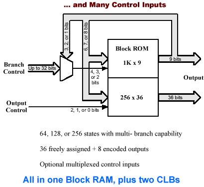
Other, more specialized uses of a block ROM are:- 20-bit binary counter, or 18-bit binary up-down counter in one block ROM, configured 1K x 18, running up to 200 MHz. - Six-digit BCD counter in one block ROM, configured 512 x 36, plus one CLB, running up to 300 MHz. These counters use one port for the less significant half of the counter, and the other port for the more significant half. This is possible because the count algorithm, stored in the ROM, is common to both halves. - Two independent 11-bit binary to 4-digit BCD converters, with the block ROM configured 1K x 18 and the LSBs not passing through the converters. - Two independent 3-digit BCD to 10-bit binary converters, with the block ROMs configured 2K x 9 and the LSBs not passing through the converters. - Sine-cosine look-up tables using one port for sine, the other one for cosine, with 90 degree-shifted addresses, 18-bit amplitude, 10-bit angular resolution. - u-law to/from A-law telephony code converter, or u/A-law to linear converter. The Virtex-II user is encouraged to analyze any design for leftover multipliers and block RAMs, and use them to unburden the logic fabric where possible. Using multipliers as shifters and block RAM as state machines also simplifies the design effort, significantly reduces routing overhead and power consumption, and achieves higher performance: It is hard to beat this combination, especially when it comes for free! |
||||||||