
A Current Sensing TutorialPart II: Devices
3 comments
After reading this series of articles on current sensing, you will have a solid grasp of the fundamentals of current sensing, devices that are used for current sensing, how to calculate the accuracy of a solution, and guidelines for printed circuit board (PCB) layout and troubleshooting. This article introduces the four differential amplifiers that typically are used in direct current sensing solutions: operational amplifiers (op amps), difference amplifiers (DA), instrumentation amplifiers (IA), and current shunt monitors (CSM).
Operational amplifiers
The use of an op amp for current sensing is limited by input common-mode voltage. Due to the design of the input stage, input common-mode voltage of such a device is limited by the supply voltage (Voa). Additionally, the large open-loop gain of a traditional op amp requires the device to have feedback, which limits its use to single-ended input signals. Such a configuration necessitates its use to only low-side current sensing. Figure 1 depicts the use of an op amp in a low-side current sensing configuration.
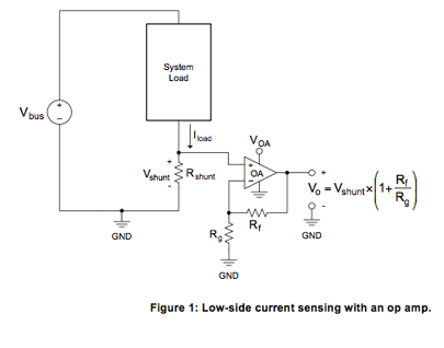
Since the input common-mode voltage of the solution shown in Figure 1 is near ground, the op amp input common-mode range should include ground. It may also be desirable to select an op amp whose output is considered rail-to-rail. This yields the greatest range of load currents that can be accurately sensed. One drawback is any parasitic resistance between the shunt resistor and the ground trace adds to the shunt resistor value (see Figure 2).
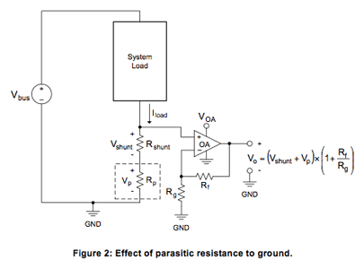
The voltage developed by a parasitic resistance in this location (for example, PCB trace, solder joint) will pedestal the shunt voltage, thereby introducing error. This parasitic resistance may vary greatly in production. For greater accuracy and consistency, a differential measurement across the shunt resistor is required.
Difference amplifiers
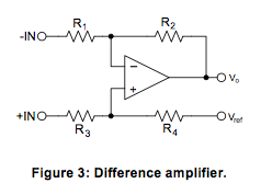
A traditional DA is simply an op amp with a precision trimmed resistor network as shown in Figure 3. The resistors are typically trimmed during manufacturing so that R2/R1 = R4/R3. The differential gain (Adm) of the device is therefore R2/R1. The reference voltage (Vref) is added to the output voltage (Vo).
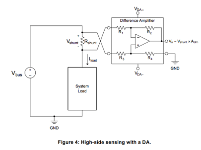
With respect to current sensing, a DA can have input common-mode voltages outside of the supply voltages due to the resistive divider at the inputs, as shown in Figure 4. This allows one to use a DA for high-side current sensing. However, a DA places a load on the system bus voltage due to its finite common-mode and differential-mode input impedances. This load draws current from the system bus voltage, which introduces uncertainty in the measurement. In order to reduce the measurement error due to these input impedances, they should be significantly larger than the system load impedance.
Since the common-mode voltage of a low-side current sensing solution is near 0V, a DA can be used as shown in Figure 5. This minimizes the effect of the common-mode input impedance, but the differential-mode input impedance is still a factor. The use of a DA for low-side measurements negates the issue caused by parasitic resistance to ground in series with the shunt resistance that was discussed in the op amp section. Finally, DAs have fixed differential gains because the resistor network must be trimmed to maintain good common-mode rejection ratio. Some DAs have an on-chip non-inverting amplifier whose gain can be adjusted. If other gains are required it is advisable to either select such a device or add gain to the output of the DA with an external op amp circuit.
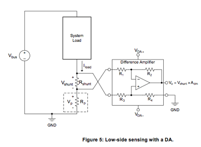
In summary, a DA can be utilized for either high-side or low-side sensing. When used for high-side sensing, error can be introduced by the finite common-mode and differential-mode input impedances. When used for low-side sensing, a DA can negate the issue caused by any parasitic resistance to ground that is in series with the shunt resistance.
Instrumentation Amplifiers
Instrumentation amplifiers are typically composed of a DA output stage with buffered inputs as shown in Figure 6.
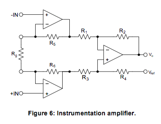
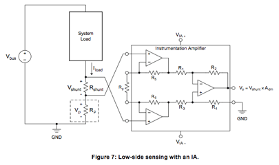
The first advantage over a DA is the ability to easily change the differential gain (Adm) of the device using an external resistor (Rg). Secondly, the inputs are connected to the non-inverting inputs of a buffer amplifier. The non-inverting inputs are high-impedance, which translates to almost no load on the system bus voltage allowing for the sensing of small system currents. One disadvantage, however, is that the input common-mode voltage of IAs is limited by their supply voltage. Therefore, IAs typically is utilized for low-side measurements (Figure 7).
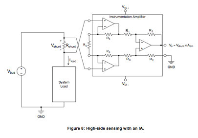
It is possible to utilize an IA in a high-side measurement (see Figure 8). The designer must ensure that the system bus voltage is within the input common-mode range of the IA as dictated by its supply voltage.
Current shunt monitors
Current shunt monitors are devices that place little load on a system and allow for sensing current under high common-mode voltage conditions. This ability is gained through the design of unique input stages. A typical op amp common-emitter input stage is depicted in Figure 9, while a common-base input stage of a CSM is depicted in Figure 10.
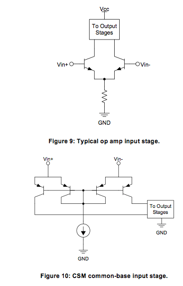
To illustrate this benefit, lets look at an example where we compare a DA and a CSM for a high-side measurement (Vcm=70V).
Current Sensing-Part II
One possible CSM solution includes the INA282, whose input common-mode range extends from 16V to 80V. At Vcm=70V, the input bias current is ~25 µA. One possible DA solution includes the INA146. The INA146 can accept input common-mode voltages of ±100V with ±15V supplies. The common-mode input impedance of the device is 55kΩ. Therefore the device will draw 70V/55 kΩ = 1.27mA from the bus supply. This comparison illustrates that a CSM can yield higher accuracy (or greater load current range) at large common-mode voltages.
As illustrated by the same example, DAs can have greater common-mode voltage ranges than CSMs.
Finally, in order to maintain good common-mode rejection ratio and desirable pricing, CSMs typically have fixed gains. The exceptions include current output devices, which require an external precision resistor to set the gain, and digital devices.
Directionality
Solutions for bidirectional load currents include most DAs, IAs, and CSMs. The datasheet typically indicates whether or not a device can be used in a bidirectional system. One key indicator of bi-directionality is the availability of a reference input, as shown in the DA and IA schematics in Figures 3 and 6, respectively. Placing a voltage on the reference pin of a device references the output to that voltage, as discussed in Part 1 in this series.
Input and output voltage range
Care must be taken to ensure than the input and output voltage ranges of all devices mentioned in this article are within the datasheet specifications. The ranges are listed in the recommended operation conditions table of their datasheets. Violating the input range of a device, at least, ensures nonlinear operation. Exposing a devices inputs to voltages outside of datasheet recommendations can also damage the device depending on duration and severity. The output range of a device is directly dependent on the supply voltages. One must ensure that the product of the input voltage and the gain of the device/circuit are within the output range specification of the device.
This is especially important when selecting the supply voltage for IA solutions. Traditional three op amp IAs, as shown in Figure 6, typically have a plot in the datasheet that shows the output voltage range versus input common-mode range for different supply conditions. An example is shown in Figure 11.
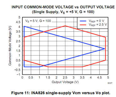
If the INA826 is used for a low-side measurement (Vcm ≈ 0V), the output voltage range of the device extends only from ~0.1V to ~1.2V when Vs = 5V (single-supply), Vref = 0V, and G = 100. This range may be too restrictive to utilize the full input range of a typical ADC.
Powering the device with dual supplies, however, allows for a larger output voltage range, as shown in Figure 12.
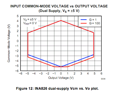
Vs = ±5V allows the output to swing from 4.9V to +4.85V when Vcm=0V for gains of 1 or 100. However, depending on the system and application, this may require the addition of a 5V power supply.
Nontraditional IAs such as the INA326 utilizes a unique topology that enables true rail-to-rail input and output voltage ranges. With a single-supply voltage of 5V, the INA326s input voltage range is 20 mV to 5.1V. The output voltage range can swing to within 75 mV of either supply rail. This makes such devices attractive for low-side current measurements.
Summary
In summary, we have presented the four devices that typically are utilized for direct current sensing: op amps, DAs, IAs, and CSMs. It was found that RRIO op amps are useful for low-side current sensing. Difference amplifiers, however, can be used for high-side current sensing in the presence of high common-mode voltages at the expense of drawing current from the system bus supply. They can also be used for low-side sensing and negate the effects of parasitic resistances to ground. Instrumentation amplifiers, like op amps, are limited to common-mode voltages within their power supplies and are generally used for low-side sensing.
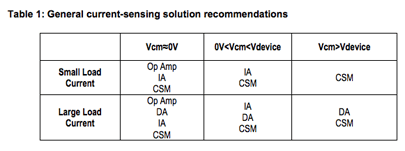
Finally, CSMs employ unique input stage topologies that allow for a wide range of common-mode voltages while placing less of a load on the system than a DA. Most CSMs can be used for either high or low-side sensing. Table 1 provides general solution recommendations based on the devices supply voltage (Vdevice) with respect to the systems bus voltage, or Vcm, and the magnitude of the load current.
In the next article, we will examine the accuracy of a solution. Specifications such as common-mode rejection ratio (CMRR), power supply rejection ratio (PSRR), and initial input offset voltage (Vos) will be introduced.
References
For answers to current sensing applications questions please visit TIs Precision Amplifiers forum in the E2E community.
The complete series
- A Current Sensing Tutorial--Part 1: Fundamentals
- A Current Sensing TutorialPart II: Devices
- A Current Sensing Tutorial--Part III: Accuracy
- A Current Sensing TutorialPart IV: Layout and Troubleshooting Guidelines
About the Authors
Peter Semig is an Applications Engineer in the Precision Linear group at TI where he supports difference amplifiers, instrumentation amplifiers, and current shunt monitors. Peter received his BSEE and MSEE from Michigan State University, East Lansing, Michigan. If you have questions about this article, contact Peter at ti_petersemig@list.ti.com.
Collin Wells is an applications engineer in the Precision Linear group at TI where he supports industrial products and applications. Collin received his BSEE from the University of Texas, Dallas.
