A Current Sensing Tutorial--Part III: Accuracy
Post a comment
After
reading this series of articles on current sensing, you will have a solid grasp
of the fundamentals of current sensing, devices that are used for current
sensing, how to calculate the accuracy of a solution, and guidelines for printed
circuit board (PCB) layout and troubleshooting. This article investigates some
of the specifications that affect a solutions accuracy. These specifications
include input offset voltage (Vos), common-mode rejection ratio (CMRR), and
power supply rejection ratio (PSRR).
Accuracy
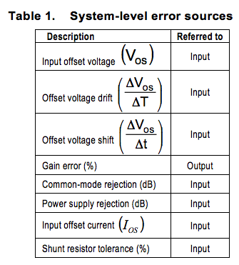
The system accuracy of a current shunt measurement is impacted by a plethora of error sources including those shown in Table 1. Worst-case system accuracy is defined as shown in Equation 1.

Where is the error contribution (%) of each error source. A more probable approach to calculating system accuracy, however, is to combine uncorrelated errors in a root-sum-square (RSS) fashion as shown in Equation 2.


Since most of the errors listed in Table 1 are referred-to-input (RTI), it is advantageous to discuss accuracy with respect to the input. Errors that are referred to the input of the device can be multiplied by the device gain to determine their contribution at the output.
Input offset voltage
Input offset voltage is typically the largest factor affecting a solutions accuracy. It is defined as the DC voltage that must be applied between the input terminals to force the quiescent DC output voltage to zero or some other level, if specified. [1] An amplifiers ideal Vos is 0V. Process variations and device design constraints, however, cause non-zero values of Vos.
All input-referred errors are calculated with respect to the ideal shunt voltage. The ideal shunt voltage is the product of the load current and ideal shunt resistor value. Lets calculate the error contribution of a devices Vos specification in a system whose nominal load current is 5A and ideal shunt resistor value is 1m?, shown in Equation 3. Assume that we have decided to use the INA170, whose maximum Vos specification is 1mV.

In order to decrease this error, we have two options: increase the Rshunt resistance or decrease Vos(max). Increasing the Rshunt resistance may or may not be feasible due to cost, board space, or power dissipation. Alternately, we could try to find a substitute device with lower Vos.
Finally, note the inverse relationship between load current and error. In our example, we calculated 20 percent with a nominal load current of 5A. If the system load current decreases, the contributed error due to the Vos specification increases. Therefore, a designer should calculate worst-case error at minimum load current.
Common-mode rejection ratio
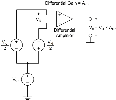
Before introducing CMRR, the concept of input common-mode voltage needs to be revisited. As discussed is the first article in this series, the input common-mode voltage of an amplifier is defined as the average voltage common to both input terminals. While this is strictly true, it is convenient to separate the voltage across the shunt from the common-mode voltage. This can be accomplished by defining Vid, or differential input voltage. In current sensing applications this can also be thought of as the shunt voltage. Figure 1 provides an alternate definition of input common-mode voltage that introduces the differential input voltage. Figure 1 also reintroduces the concept of differential mode gain (Adm). The ideal output of a differential amplifier is the product of the differential input voltage and the differential mode gain.

Figure 1: Alternate definition of common-mode voltage [2]
CMRR can affect a current sensing solutions accuracy. It is a measure of a devices ability to reject common-mode signals. This is important because common-mode signals can manifest themselves inside a device as differential signals, thereby decreasing the accuracy of a solution.
CMRR is typically specified in product datasheets on either a linear scale (?V/V) or a logarithmic scale (dB). If reported in dB, the worst-case value is the minimum value. If reported in µV/V, the worst-case value is the maximum value.
In order to calculate the error due to a devices CMRR specification, we need the following: worst-case CMRR specification from the datasheet, common-mode voltage test condition from the datasheet specification table (Vcm-pds), and the systems common-mode voltage (Vcm-sys).
For example, assume we have a system whose common-mode voltage is 50V (Vcm-sys) and shunt voltage is nominally 5mV. Lets calculate the error using the INA170, whose worst-case CMRR specification is 100dB (min) and Vcm-pds=12V.
Since the specification is given in dB, we need to convert it to a linear scale, as shown in Equation 4.

Now we calculate the error as shown in Equation 5.

In order to decrease the error contribution due to CMRR we have two options: increase the shunt voltage or select a device with better CMRR performance. Changing Vcm-sys is not usually a realistic option for it is dictated by the application.
This treatment of CMRR is meant to give the reader a quick and useful understanding of how it affects the accuracy of a measurement [1, 3, 4].
Power supply rejection ratio
PSRR is a measure of the change in Vos created by a change in power supply voltage. Error due to PSRR can be calculated in a manner similar to CMRR.
In order to calculate the error due to a devices PSRR specification, we need the following: worst-case PSRR specification from the datasheet, supply voltage test condition from the datasheet specification table (Vs-pds), and the supply voltage that will power the device in the system (Vs-sys).
For example, the INA170 has a worst-case PSRR specification of 10?V/V(max) with Vs-pds=5V. If the device is actually supplied with 30V (Vs-sys), the error due to PSRR is calculated as shown in Equation 6. As with the previous examples we assume a shunt voltage of 5mV.

In order to decrease the error contribution due to PSRR we have two options: increase the shunt voltage or select a device with better PSRR performance. Changing Vs-sys is not usually a realistic option for it is typically dictated by the application.
In this particular example, PSRR was already specified in µV/V. If the value was specified in dB it must be converted to a linear scale before applying Equation 6.
Other errors
Some specifications, such as gain error and shunt resistor tolerance, are typically given in percentage form. This makes their incorporation into an accuracy calculation straightforward.
Table 1 also lists Vos drift and shift. Input offset voltage drift measures the change in Vos due to a change in temperature. This specification is typically

Input offset voltage shift, however, is not as straightforward. Input offset voltage shift measures the change in Vos due to a change in time. This specification is not usually found in a datasheet and can only be estimated. One way to approximate shift is to understand that a devices Vos can shift by an amount no greater than the devices maximum Vos specification over a 10-year period. This shift is in addition to the devices initial Vos specification.
Current Sensing--Part III
Putting it all together
As mentioned earlier, each of the error terms can be combined to determine a systems overall accuracy. Simply adding each term yields the worst-case error while combining them in a RSS fashion yields a more probable scenario.
For the Vos, CMRR, and PSRR examples given in this article the worst-case accuracy would be 67.4% as shown in Equation 7.

Combining the errors in a RSS fashion yields a more probable accuracy of 78.03% as shown in Equation 8.

Summary
This article defined the concept of current sensing accuracy as it relates to specifications such as Vos, CMRR, and PSRR. Examples were given on how to calculate errors caused by these specifications in a particular application. Other errors such as gain error, shunt tolerance, and Vos shift and drift were also briefly discussed. The final article in this series will discuss current sensing PCB layout and troubleshooting guidelines.
References
1. Karki, Understanding Operational Amplifier Specifications, White Paper: SLOA011, Texas Instruments, 1998.
2. Tobey, Graeme, Huelsman, Operational Amplifiers: Design and Applications, McGraw-Hill, 1971.
3. Franco, Design with Operational Amplifiers and Analog Integrated Circuits, 3rd Edition, McGraw-Hill, 2001.
4. Frederiksen, Intuitive Operational Amplifiers: From Basics to Useful Applications, Revised Edition, McGraw-Hill, 1988.
For answers to current sensing applications questions, visit TIs Precision Amplifiers forum in the E2E community: http://www.ti.com/general/docs/lit/getliterature.tsp?literatureNumber=sloa011&fileType=pdf.
The complete series
- A Current Sensing Tutorial--Part 1: Fundamentals
- A Current Sensing TutorialPart II: Devices
- A Current Sensing Tutorial--Part III: Accuracy
- A Current Sensing TutorialPart IV: Layout and Troubleshooting Guidelines
About the Authors
Peter Semig is an applications engineer in the Precision Linear group at TI where he supports difference amplifiers, instrumentation amplifiers, and current shunt monitors. Peter received his BSEE and MSEE from Michigan State University, East Lansing, Michigan. If you have questions about this article, contact Peter at ti_petersemig@list.ti.com.
Collin Wells is an applications engineer in the Precision Linear group at TI where he supports industrial products and applications. Collin received his BSEE from the University of Texas, Dallas, Texas.
