
A Current Sensing TutorialPart IV: Layout and Troubleshooting Guidelines
8 comments
Input Bias Current
Before introducing the effects of PCB layout on accuracy, the input bias current specification (Ib) must be understood. Input bias current is defined as "The average of the currents into the two input terminals with the output at the specified level."[1] Ideally this specification is 0A, but process variations and design constraints cause this to be a non-zero value. With respect to current sensing, this specification has two implications. First, Ib becomes important when trying to accurately sense small currents. For example, attempting to measure a system load current of 100uA with a device whose Ib=35uA would yield great uncertainty in the measurement. Secondly, poor matching between the two input signal currents (or input offset current, Ios) could induce and/or exacerbate a differential voltage at the inputs of the device. The latter will be discussed in this article.
Theory
Part 3 in this series discussed accuracy with respect to device specifications such as Vos, CMRR, and PSRR. It also presented and discussed a table similar to the one depicted below. The differences include the addition of two rows and one column. Rows for Ib and offset voltage due to PCB layout (Vos-pcb) have been added. A column designating whether or not each error source is within the control of the designer was also added.
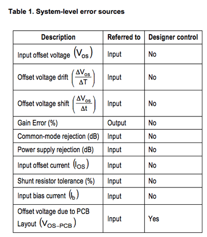
Notice that the only error source that is within the control of the designer is Vos-pcb. This is because all of the other error sources are device specifications, which cannot be realistically controlled outside of selecting a different device with improved specifications. Vos-pcb can be minimized through proper PCB layout. Unfortunately it is often the case where the appropriate device is selected, but the PCB layout causes an unacceptable amount of additional error.
Example Design
In order to observe the effects of PCB layout on a current sensing solution, lets create an example design. Suppose the solution requirements are as follows:
* Common-mode voltage (Vcm): 70V
* Available supply for differential amplifier (Vs): 5V
* Load current range: 5A<Iload<10A
* Unidirectional
* High accuracy
Since the common-mode voltage is considerable and greater than the supply voltage available for the differential amplifier, a current shunt monitor (CSM) should be the device of choice. The INA282 (Gain=50V/V) CSM meets the above requirements for it can accommodate common-mode voltages up to 80V, operate on supply voltages from 2.7V to 18V, can be used in either bidirectional or unidirectional applications, and has an input offset voltage (Vos) specification of only 70µV(max).
In order to properly size the shunt resistor we must examine the input and output specifications of the device. With a supply voltage of 5V, the output of the INA282 can swing from 40mV to 4.6V. Dividing the output range by the gain of the device (50V/V) yields the input range. This equates to an input voltage range from 0.8mV to 92mV.
Given our load current of 5A (Iload-min) to 10A (Iload-max), the shunt resistor must be smaller than 9.2mO (92mV/Iload-max) and larger than 0.16mO (0.8mV/Iload-min). If the power dissipation of the shunt resistor is tolerable, it is recommended to use a larger valued shunt resistor for accuracy purposes. Therefore, we will select a shunt resistor of 8mO.
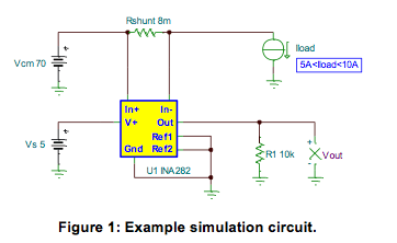
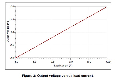
Figure 1 depicts the TINA-TI simulation circuit used to verify the design. Figure 2 shows the output of the INA282 vs. load current.
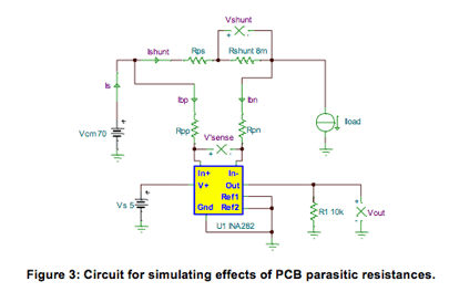
Now that we have a working example, lets look at the effects PCB layout can have on the accuracy of this solution. Figure 3 depicts the same circuit as Figure 1, but with the addition of the parasitic resistances (Rps, Rpp, and Rpn). It also differentiates between the shunt voltage (Vshunt) and the sense voltage (Vsense). Vsense is defined as the differential voltage at the input pins of the device. Ideally, Vshunt=Vsense. Due to PCB parasitics, however, this will not be the case. Therefore, Vsense represents the non-ideal sense voltage.
Similar to our previous accuracy discussion, the error due to the PCB layout can be defined as shown in Equation 1.

where Vos-pcb is defined as:

From Figure 3 we can also derive an equation for Vsense in terms of the parasitic resistances and bias currents.
By Kirchoffs current law (KCL):

By Kirchoffs voltage law (KVL) and the passive sign convention:

Solving for Vsense yields:

Equation 6 shows us that any parasitic resistance in series with the shunt resistor, Rps, induces an error that will be observed at the output of the current sensing device. It also shows that parasitic resistances in series with the inputs of the current sensing device, Rpp and Rpn, may or may not induce an error. If Ibp*Rpp=Ibn*Rpn, no error will be observed. Any deviation from this relationship will induce error.
Rpn and Rpp errors
While the system designer cannot control the input bias currents, they can attempt to match the resistances of the input traces. Failure to balance the input trace resistances will most likely be perceived as an error.
For example, one-ounce copper input traces of 350mils in length and 10mils wide have an impedance of approximately 17mO. Table 2 summarizes the effects of such input traces on the circuit from Figure 3 with a load current of 5A.

Using the ideal shunt voltage value of 40mV, we calculate the error due to balanced input traces using Equations 1, 2 as follows:

Failure to balance the input traces, however, can yield a more significant error. Lets repeat the calculations but use imbalanced traces. Lets assume one of the traces is 275mils in length while the other is 350mils long. The results of the simulation are shown in Table 3.
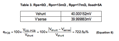
We see a 35.7 percent increase in error with a 75mil imbalance. Two additional topics to mention here include temperature variations and vias. These errors can increase further due to temperature fluctuations. Additionally, placing the current sensing device and the shunt resistor on opposite sides of the board necessitate the use of vias. Vias can have significant parasitic impedances which can vary greatly with manufacturing.
Current Sensing--Part IV
Though the error is small, the idea of canceling the effects of unbalanced input bias currents by purposefully misbalancing the input traces is neither practical nor recommended. The difference in input bias currents will vary part-to-part, wafer-to-wafer, and lot-to-lot. It can also vary based on design parameters such as common-mode voltage and supply voltage.
Therefore, it is recommended to place the current sensing device and shunt resistor on the same side of the PCB board and to use balanced, short input traces.
Rps Errors
As shown in Equation 6, parasitic trace resistance in series with the shunt resistor can induce measurement error. In this scenario, the parasitic resistance is in the high current path. Therefore, it does not take a significant amount of parasitic trace resistance to cause significant error.
For example, a one-ounce copper trace of 10mils in length and 25mils wide has an impedance of approximately 193µΩ. While this may not seem significant, please recall that it can carry the maximum load current (10A). Table 4 summarizes the effects of such input traces on the circuit from Figure 3 with a load current of 10A.

Using the ideal shunt voltage value of 80mV, we calculate the error due to Rps using Equations 1 and 2 as follows:

Equation 9 depicts the importance of removing all parasitic resistance in series with the shunt resistor. This can be accomplished by implementing a Kelvin-connection between the shunt resistor and the current sensing device, which will be discussed in the section on Layout Recommendations.
While this error is clearly more significant than the errors caused by Rpp and Rpn, an additional observation can be made: it is possible to measure a larger voltage at the input pins of a current sensing device than across the shunt resistor. Consequently, a larger voltage will be observed at the output of the device.
This observation is important when troubleshooting a current sensing solution. It is common for one to measure the voltage across the shunt resistor, multiply it by the nominal gain of the device, and compare the result to the measured output of the device. In this case, the ideal shunt voltage is 80mV, the nominal gain of the device is 50V/V, and the simulated output is 4.084V. The product of the shunt voltage and nominal gain is 4V. The 84mV discrepancy (or 2.1% error) could lead one to believe the devices gain error is not within specification.
The error introduced by the device itself, however, can be calculated using Equations 10 and 11:

The use of Vsense for this calculation eliminates any error induced by the PCB layout and reports only the error introduced by the device itself.

We see the error contributed by the device is actually 0.3% when Vsense is used for the calculation, which is significantly less than when using Vshunt. When troubleshooting a current sensing solution, it is imperative to measure the voltage at the input pins of the device instead of the shunt voltage.
Layout recommendations
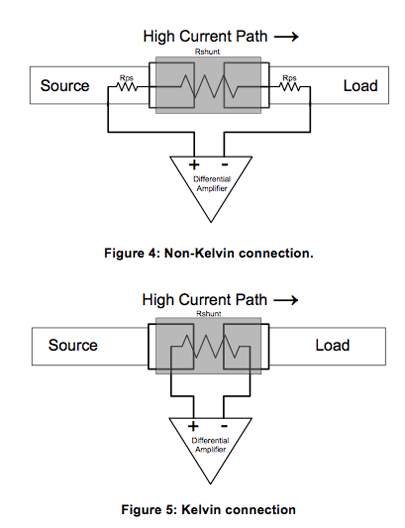
It has been shown that any parasitic resistance in series with the shunt resistor will induce an error. Therefore, it is recommended that the designer implement a Kelvin-connection between the shunt resistor and the current sensing device. Non-Kelvin and Kelvin connected layouts are shown in Figures 4, 5, respectively.
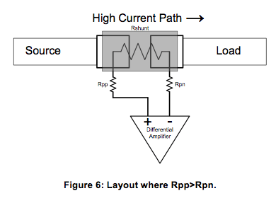
As discussed earlier, it is recommended that the input traces are short and balanced. Figure 6 depicts a layout such that Rpp>Rpn.
Summary
We showed that parasitic resistances either in series with the shunt resistor or in series with the input pins of a current sensing device can induce measurement errors. In order to minimize such errors, it is recommended to Kelvin-connect the shunt resistor and use short, balanced traces for the input connections. Finally, care should be taken when calculating device error. It is recommended to take all device-related measurements at the pins of the device as opposed to other convenient locations, such as test points or across the shunt resistor itself.
References
1. Karki, James. Understanding Operational Amplifier Specifications, White Paper (SLOA011), Texas Instruments, 1998.
For answers to current sensing applications questions, visit TIs Precision Amplifiers forum in the E2E community.
Download a free copy of TINA-TI here.
The complete series
- A Current Sensing Tutorial--Part 1: Fundamentals
- A Current Sensing TutorialPart II: Devices
- A Current Sensing Tutorial--Part III: Accuracy
- A Current Sensing TutorialPart IV: Layout and Troubleshooting Guidelines
About the Authors
Peter Semig is an Applications Engineer in the Precision Linear group at TI where he supports difference amplifiers, instrumentation amplifiers, and current-shunt monitors. Peter received his BSEE and MSEE from Michigan State University, East Lansing, Michigan. If you have questions about this article, contact Peter at ti_petersemig@list.ti.com.
Collin Wells is an Applications Engineer in the Precision Linear group at TI where he supports industrial products and applications. Collin received his BSEE from the University of Texas, Dallas.
