|
Does Real Time
debugging really just make you wait?
For years, designers
have been taking advantage of the time-to-market benefits of designing
their systems using Xilinx programmable logic devices. Now, Xilinx has
made it even easier to beat your competition to the market by accelerating
the process of in-system verification using PROBE.
PROBE is an interactive
tool that simplifies the process of observing the behavior of signals within
an FPGA while operational in a target system. As a result
of the PROBE operation, you are able to use your existing test equipment
to analyze the circuit's behavior in a manner that is familiar to you.
Xilinx began shipping
PROBE as part of its Alliance and Foundation Series tools starting with
the v2.1i products. The following sections show you how to take advantage
of PROBE.
PROBE
Benefits
As part of a larger
suite of verification tools, PROBE is the most efficient tool for selecting
internal signals as test points during board level analysis. Once these
signals are brought out as test points, you can use your existing lab equipment
to most efficiently debug your design. You do not have to learn how to
operate new tools, so you can leverage your existing knowledge. Furthermore,
you avoid the complications of linking the trigger points of your existing
equipment to additional analysis tools.
PROBE also provides
you with the ultimate flexibility to identify the signals you want to analyze.
Given a set of reserved test points, you simply modify the signals you
want to view on your logic analyzer (or oscilloscope) using the intuitive
Graphical User Interface (GUI). With a push of a button, PROBE quickly
completes the task of routing the chosen signal to your PROBE point. In
many cases, you can merely leave your test leads on the boards test points,
and use PROBE to quickly and efficiently view different signals without
having to touch the test equipment.
How
to Use PROBE
Using PROBE to debug
your design is easy!
When you are creating
your design, route the spare I/O from your Xilinx device to test points
on your Printed Circuit Board. This makes it easy to attach test leads
to these signal traces, and in circumstances where additional functionality
is added to the Xilinx device, it also makes it easier to "blue wire" external
signals to the chip as well.
Once you begin debugging
the design and find that you need to look at a signal that is internal
to the Xilinx device, it is a simple matter to identify this signal and
the desired test point from within the PROBE dialog box. To start, open
the design you want to test within the Xilinx FPGA Editor.
The following steps
will show you how to use PROBE.
| 1) Invoke
PROBE's dialog box using the simple toolbar menu pick. |
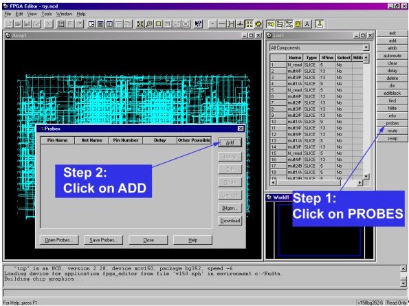 |
| 2) Select
Add within the PROBE dialog box. |
|
|
| 3)
Next, assign the PROBE name. |
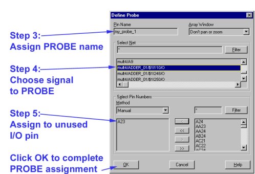 |
| 4) Choose the desired
signal using the "Select Net" filter and browse function. |
| 5) Assign
the selected signal to a PROBE pin. |
| 6) Push
OK to have PROBE assign the signal to the device pin.
Of course, PROBE
can assign multiple test points during each assignment operation (limited
to the number of I/O reserved for PROBE's use). |
|