

|
|
| |
|
Answers Database
CONCEPT-HDL: How to generate a board-level symbol?
Record #1728
Product Family: Software 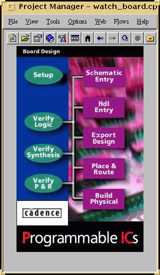 Cadence Project Manager From the Cadence Project Manager, select "Setup" -> "Tools" -> "Programmable IC" -> "Setup" -> "Xilinx" -> "Setup" to launch the "PIC Setup" window for Xilinx. 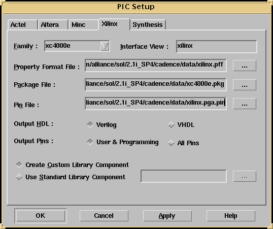 PIC Setup Select the target device family. The fields for "Property Format File", "Package File", and "Pin File" are automatically filled-in for you if the XILINX environment variable is properly set. You can use either use a standard library component or create a custom component for the design implemented. Choose the Create Custom Library component option, Concept-HDL creates a separate cell with the following views: Sym_1, Chips, and Entity. Next, select "Place & Route" from the Cadence Project Manager. Enter the path of the EDIF file. This will create the Xilinx view. 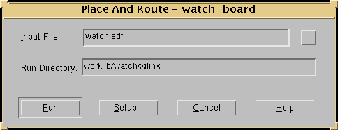 Place and Route Input From the Xilinx Design Manager, select "Design" -> "Options". Select "Generic Verilog" as the simulation template, and click on "Edit Options". For the "General" tap, change the "Simulation Netlist Name" to <design>_routed. Where <design> is your design name. 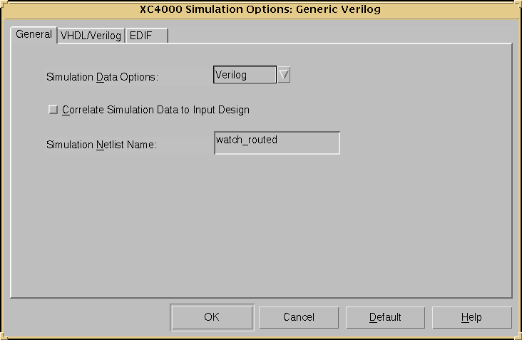 General options for Ngd2ver For the "VHDL/Verilog" tap, select the option for "Generate Pin File". 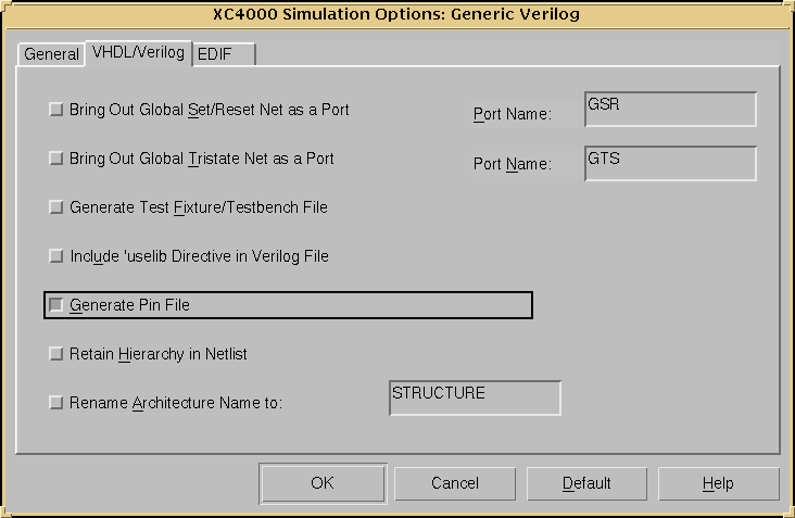 VHDL/Verilog options for Ngd2ver The Xilinx view contains an implemented Verilog file and SDF file. However, you need to copy the <design>_routed.pin to the Xilinx view. The Xilinx view exists at worklib/<design>/xilinx. From the Cadence Project Manager, select "Build Physical", and the set the appropriate location of the "Mapped Verilog Netlist" and "SDF File" that reside in the Xilinx view. 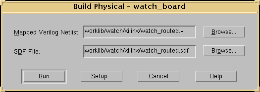 Build Physical Input The custom library component is created as a design cell named <design>_routed_1. In addition, the "Build Physical" process creates a pic_1 schematic view containing master.tag and page1.csb, allowing instantiation of this custom library component. If you use a standard library component, the pic_1 schematic view instantiates this component. Open the schematic view pic_1 in Concept-HDL and save it to obtain the netlist. You perform the build physical step after implementing the design creates a schematic view pic_1. This schematic instantiates the custom component created or the standard component selected at the time of building the physical views. While the sch_1 schematic view contains the logical design, implementation occurs in the physical device instantiated in the pic_1 view. Choose the view pic_1 for packaging the implemented design. End of Record #1728 - Last Modified: 12/22/99 17:23 |
| For the latest news, design tips, and patch information on the Xilinx design environment, check out the Technical Tips! |