|
|
 |
| Pamette is a reconfigurable computing platform that is based on the
Xilinx 4000 series FPGA. The PCI module uses a total of five FPGAs: four
user-area FPGAs for application development and one FPGA as an interface
to the PCI device. The user-area FPGAs can be dynamically loaded during
runtime and are infinitely reprogrammable. The board also contains 256KB
of SRAM, four PMC connectors for one mezzanine card and four 72-pin DRAM
sockets. The result is a board with in an infinite number of possible applications.
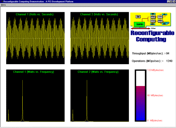
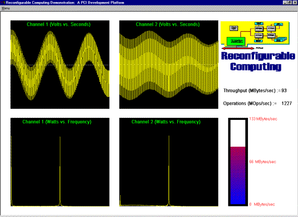
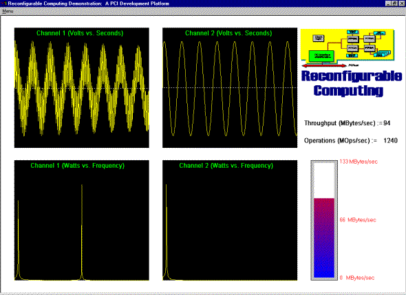
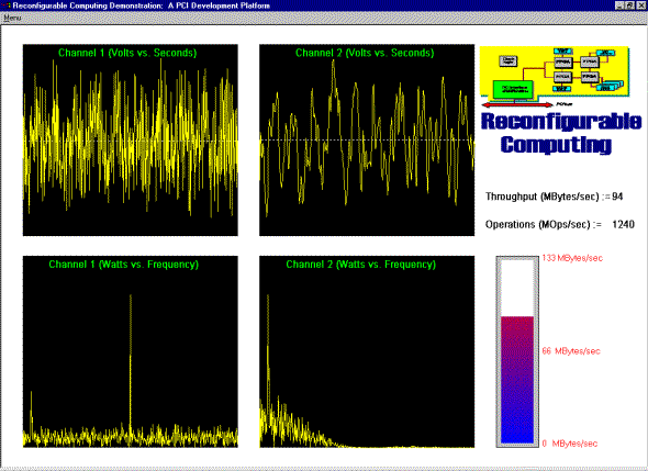
This demonstration shows the high bandwidth I/O capabilities of Pamette coupled with the benefits of pipelined data manipulation. Data is transmitted from one system and receiver in another, simulating a generic transmitter/receiver system. The user has the ability to generate the transmitted waveform and select the appropriate filter. The transmitted waveform consists of two sinusoids and a noise generator added together. These selections are made through a GUI running on Digital UNIX. The result of the transmission and filter is displayed on a system running Windows NT. The time and frequency domain is displayed for the two transmitted channels. One channel is filtered, while the other is simply passed. The FFT of each channel performed by the systems Alpha processor. Two custom daughter cards were designed to create an LVDS link between the two systems The Each card contains deep programmable FIFOs. As data is passed from the daughter card through user FPGAs to the PCI interface chip, it is filter using standard FIR techniques (see figure above). (It is important to point out that the board is not limited to FIR filters.) The demo currently has two 16-bit channels, but the Pamette board and accompanying daughter card can handle up to four 16-bit channels. In this case, 32 operations are performed on each channel on every clock tick. The computational power of the board in this configuration is 2112 million operations per second. These operations reduce the computational pressure put on the system CPUs. Data decimation can also reduce memory requirements and computation cycles. The demonstration uses page mapped DMA to reduce the number of interrupts, resulting in a higher net bandwidth. DMA rates are consistently above 100 MB/s. A 64-bit upgrade is planned which should push the rates to 200 MB/s. Both the receiver and transmitter side of the demo consisted of a Pamette card and a unique accompanying daughter card. The previously mentioned bandwidth numbers were exceeded on both the transmitter and receiver. The transmitter reads system memory and the receiver writes to system memory. Facts:
The demonstration use both Digital UNIX and Windows NT.
|