The XilinxÒ VirtexÔ -E Family:
Bandwidth Solution for Next Generation High Performance Systems
A Product Backgrounder

Introduction

With the introduction of the Virtex series, Xilinx redefined the field programmable gate array (FPGA). Unparalleled density and performance coupled with a powerful set of system level features enabled designers to architect their systems with the Virtex capabilities at the core. 

As a result of being designed in system critical applications, the measuring criteria of an FPGA has grown from the traditional measurements of density and performance to include bandwidth capability. Bandwidth is the measure of how many actions can be accomplished in a given amount of time and is the key differentiating factor for many end products. Computing architectures measured in million instructions per second (MIPS) and data communication systems measured in gigabits per second (Gbps) highlight the importance of bandwidth.

The new Virtex-E family of FPGAs is built on the highly successful Virtex architecture. Leveraging the 0.18-micron, six-layer metal technology, Virtex-E devices push the traditional FPGA measurements to over three million gates, 804 I/Os and over 311 MHz performance. Combined with system level features for clock management, multiple standard I/O, and embedded dual port memory, the Virtex-E family is designed to support the bandwidth requirements of next generation high performance systems.

Device
Logic Cells
Dual-Port Block Memory (Kbits)
Maximum
Usable I/O
I/O 
Bandwidth (Gbits/sec)
XCV50EÔ
1728
56
176
44
XCV100EÔ
2700
80
176
44
XCV200EÔ
5292
112
284
71
XCV300EÔ
6912
128
316
79
XCV400EÔ
10800
160
404
100
XCV600EÔ
15552
288
512
127
XCV1000EÔ
27648
384
660
164
XCV1600EÔ
34992
576
724
180
XCV2000EÔ
43200
640
804
200
XCV2600EÔ
57132
736
804
200
XCV3200EÔ
73008
832
804
200
The Virtex-E family consists of the 50,000-gate XCV50E device
to the industry's first FPGA to exceed three million gates, the XCV3200E device.

I/O Bandwidth Scalable to 200 Gbps

The I/O bandwidth is calculated by multiplying 311 MHz I/O performance rate times 80 percent of the maximum usable I/O number—where 80 percent is the assumption used for a typical percentage of the device's I/Os used as data signals. It is very likely that a given design will require multiple high bandwidth data ports with the bandwidth distributed across the required ports. For next generation systems, port bandwidth on the order of 10 Gbps such as OC-192 data rates is the leading edge. With the high bandwidth capability supported by the Virtex-E architecture, several 10 Gbps ports can be achieved within a single device.

Bandwidth Enabling Technology

Simply having input and output pins that can toggle at high frequencies is only one part of the complete solution for addressing next generation bandwidth requirements. Precise clock management that controls timing relationships between external clock and data must allow the device to interface with a variety of external components with some flexibility. Once the high bandwidth is captured at the device pins, capabilities for internal memory and logic must process the data at the required bandwidth. Furthermore, to communicate with external interfaces (such as with high-speed external memory or system backplanes) the device pins must address a variety of signal standards. The Virtex-E devices contain advanced system technology to support the bandwidth requirements throughout the system. The illustration below shows a block diagram of the Virtex-E bandwidth enabling technology including 100 percent digital delay lock loops (DLL), True Dual-PortÔ embedded memory and SelectI/O+Ô technology to address these areas of high-bandwidth support.


Virtex-E Architecture Overview

Eight High Performance DLLs - Drop-in Bandwidth Optimization 

Supporting the highest bandwidth data rates between devices requires advanced clock management technology such as DLL. The DLL circuitry allows for very precise synchronization of external and internal clocks. Xilinx was the first to deliver DLLs in programmable logic by offering four 200 MHz DLLs in every Virtex device. The Virtex-E family takes this technology to the next level with devices containing eight DLLs capable of over 311 MHz. As a fully digital implementation, the Virtex and Virtex-E DLLs do not have the typical problems of an analog phase locked loop (PLL) including board isolation and decoupling of power and ground. Virtex-E DLLs provide precise clock edges through phase shifting, frequency multiplication, and frequency division. The precise duty cycle generation is critical for high performance applications (like Double Data Rate, or DDR) in which a slight shift in duty cycle can dramatically decrease overall system performance. 

Parameter
Value
Maximum Output Frequency 320 MHz*
Maximum Output Jitter 100 ps
Output Frequency Duty Cycle 50%+/- 100ps
* Based on Virtex-E –7speed grade product
 
Bandwidth critical specifications of the Virtex-E DLL

Maximizing Double Data Rate memory bandwidth with Virtex-E DLL

A key technique for increasing the bandwidth of a particular data port is to have signals change on both edges of a clock, commonly referred to as the Double Data Rate technique. Memory suppliers have already started to support this type of high performance technique to increase the memory bandwidth of their devices. At high frequencies, signal integrity limits the clock performance, which limits the bandwidth of the data. Bandwidth for the port is immediately doubled if the architecture can change data at each edge of a system clock. It is critical that a clock duty cycle is very precise to 50 percent for this technique. Since Virtex-E DLLs can generate clocks with a duty cycle guaranteed to be within 100 picoseconds of 50 percent; system designers can achieve the maximum memory bandwidth in the DDR application. The following diagram demonstrates how Virtex-E DLLs help achieve maximum bandwidth in a 266 MHz DDR application. 
 

Virtex-E Interfacing to a 266 MHz DDR SDRAM Memory

SelectI/O+ Technology: Flexibility, High Bandwidth, and Superior Signal Integrity

In order to meet the bandwidth requirements, electrical signals need to travel on a printed circuit board over 100 MHz, standard TTL and CMOS signal technology cannot keep pace. With the Virtex series, Xilinx pioneered the SelectI/O technology designed to support 200 MHz I/O and allow a single device to interface to any device without external converters. Virtex-E SelectI/O+ technology expands the performance and flexibility by supporting high performance I/O standards such as HSTL and SSTL at over 311 Mbps per pin. In addition, Virtex-E devices are the first programmable logic device to directly interface to differential I/O standards including LVDS, Bus LVDS (BLVDS) and LVPECL. The Virtex-E family offers a hierarchy of differential support, including up to 36 I/O pairs for LVDS and LVPECL operating at 622 MHz , and up to 344 differential pairs operating at over 311 MHz. Support for up to 344 differential pairs capable of over 311 MHz provides maximum bandwidth of over 100 Gbps, which can be distributed over the three differential signal standards as needed. For the first time in a programmable device, system designers can leverage the high bandwidth and noise immunity characteristics of these standards. 

Standard Typical Application
LVTTL 3.3 V General Purpose
LVCMOS2 2.5 V General Purpose
LVCMOS18 1.8 V General Purpose
PCI33_3 33 MHz 3.3 V PCI Backplane
PCI66_3 66 MHz 3.3 V PCI Backplane
SSTL2 (I,II), SSTL3(I,II), CTT SDRAM, DDR SRAM
HSTL(I,III,IV) SRAM, DDR SDRAM, Backplanes
GTL, GTL+, AGP Backplanes, Microprocessor Interfacing
LVDS Point to Point and Multi-drop Backplanes 
High Noise Immunity
BLVDS Bus LVDS Backplanes, High Noise Immunity, Bus Architecture Backplanes
LVPECL High Performance Clocking, Backplanes, 
Differential 100MHz+ Clocking, Optical Transceiver, High Speed Networking, and Mixed-Signal Interfacing
5 V TTL* ( 4mA Iol ) Legacy 5V TTL Interfacing
*Requires 100 Ohms external resistor
I/O standards Supported by Virtex-E Family

 
Number of Device I/O Pins 
I/O Standard Type 1 2 32 36 688 804
SSTL Single Ended 311 Mbps 622 Mbps 10 Gbps 11 Gbps 214 Gbps 250 Gbps
HSTL Single Ended  311 Mbps 622 Mbps 10 Gbps 11 Gbps 214 Gbps 250 Gbps
GTL+ Single Ended 311 Mbps 622 Mbps 10 Gbps 11 Gbps 214 Gbps 250 Gbps
LVDS Differential  n/a  622 Mbps 10 Gbps 11 Gbps 107 Gbps n/a
LVPECL Differential  n/a 622 Mbps 10 Gbps 11 Gbps 107 Gbps n/a
Bus LVDS Differential  n/a 311 Mbps 5 Gbps 6 Gbps 107 Gbps n/a
Virtex-E Aggregate Bandwidth Summary


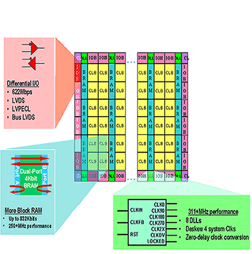
High-Performance Differential Signaling: LVPECL, LVDS, and Bus LVDS

Typical aggregate bandwidth requirements for leading edge systems are exceeding 100 Gbps. Increasingly, leading systems designers are turning to differential signaling as the mechanism of choice for these requirements. Differential signaling enables high bandwidth while reducing power, increasing noise immunity, and decreasing EMI emissions. Virtex-E devices meet this emerging challenge with unprecedented capabilities and support for high-performance differential signaling. Virtex-E SelectI/O+ technology addresses the three leading industry-standard differential signaling standards: LVPECL, LVDS, and Bus LVDS (BLVDS). 

LVPECL I/O is widely used in 100+ MHz inter-chip signaling in high-speed data communications and instrumentation systems. Fiber-Optic Network Interfaces and gigahertz Analog-to-Digital Converters, for example, rely on LVPECL I/O to achieve gigabit per second bandwidth. All Virtex-E I/Os support LVPECL input, output, and I/O signaling. This unparalleled flexibility enables users to create interfaces to hundreds of industry-standard LVPECL devices. 

In addition to high-speed interfacing, LVPECL is the industry standard for transmission of precise, on-board clocks at frequencies in excess of 100 MHz. While traditional LVTTL clock sources are typically limited to 100 MHz and below (due to the fundamental signal integrity limits), LVPECL 
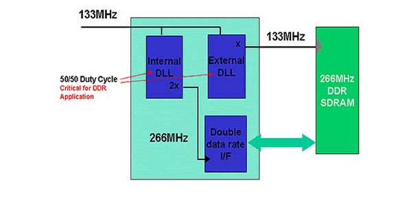
clock sources provide operation up to 400 MHz. As FPGA system clock frequencies exceed 100 MHz, LVPECL clocking becomes an essential requirement. The Virtex-E device supports high-performance LVPECL clock inputs for global and local clocking, with frequencies in excess of 300 MHz. In addition, through the use of its multiple DLLs coupled with SelectI/O+ technology, the Virtex-E devices enable zero-delay conversion of precise LVPECL clocks into virtually any required I/O standard. This facilitates the use of Virtex-E FPGAs as an integral part of high-performance board-level clock distribution strategies. 

In addition to LVPECL, the Virtex-E family has the industry’s first programmable devices to support Low-Voltage Differential Signaling (LVDS). LVDS exists in two commonly available variants, LVDS and Bus LVDS. LVDS is optimized for high-speed point-to-point links, while Bus LVDS is optimized for backplane applications employing Multi-Drop (One Transmitter, Multiple Receiver), and MultiPoint (Multiple Transmitters and Receivers) configurations. 
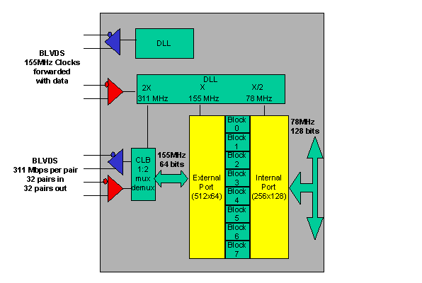
The Virtex-E device provides unparalleled support for both LVDS and Bus LVDS, with support on all devices and speed grades, and up to 688 pins (344 pairs) of LVDS and/or Bus LVDS capabilities on the largest device, providing an aggregate bandwidth in excess of 100 Gbps. The Virtex-E Bus LVDS I/Os are fully compatible with industry-standard Bus LVDS devices from National Semiconductor and other vendors. 

True Dual-Port Embedded Block Memory for Highest Internal Memory Bandwidth 

Whether used as FIFOs to buffer data on and off chip, caches for high speed parallel searches, or ATM packet buffers, the system requirements for more memory grows much faster than it does for the requirement for more logic. Xilinx pioneered using embedded distributed memory (with its SelectRAMÔ technology) in its XC4000 FPGAs to allow the configurable logic block to support logic or memory. With 
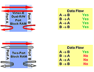
the Virtex series, this technology was enhanced to include up to 128 Kbits of True Dual-Port fast-embedded block RAM. The Virtex-E family again provides a quantum leap in internal memory bandwidth by supporting up to 832 Kbits of True Dual-Port 
RAM (208 blocks of 4Kbits memory) capable of 250 MHz performance. 


Comparison of Virtex-E True Dual-Port Memory to a Two-Port Memory

The diagram above shows that in order to emulate most of the functionality of a dual-port memory, two-port memory architectures require twice the number of memory bits and multiplexing of address and data. This results in two-port memory at roughly half the bandwidth and efficiency of the Virtex-E True Dual-Port memory in any given configuration.

Managing Bandwidth Using True Dual-Port Memory

Each True Dual-Port memory block supports 4 Kbits of memory. Each port can be configured separately to support a variety of depth/width combinations. Embedded memory can serve to buffer high bandwidth data as well as reduce the internal processing speed by transparently converting from one data width to another. The diagram below demonstrates an OC-192 application example. A data port with OC-192 bandwidth comes in on 32 BLVDS pairs running at 311 Mbits per second per pair. Eight blocks of embedded RAM are used to buffer the data internally. The port taking data from the I/O register to the memory is configured as one Kbit deep by 32. The port leading to the internal processing of the data is configured as 256 by 128. Internal processing of the 128-bit data need only run at 78 MHz to keep up with the OC-192 bandwidth. An outgoing port would be configured similarly.


Buffering the High Bandwidth Data with Virtex-E True Dual-Port BlockRAM

Completing the Solution with Packaging, Software and Intellectual Property

To support tens of gigabits per sec bandwidth through a device, the package must be capable of packing many high performance I/Os in limited board space. At the same time, package power characteristics may be required to dissipate several watts of power for the highest bandwidth applications. Virtex-E devices continue the tradition of the industry's most reliable and flexible packaging. Mainstream plastic quad flat pack (PQFP) and 1.27 mm ball grid array (BGA) as well as leading edge 0.8 mm chip scale package (CSP) and 1.0 mm fine pitch BGA (FG) are supported across the family. For the fine pitch 1.0 mm BGA offering, the Virtex-E family introduces three new FG packages: 31 mm by 31 mm FG900; 35 mm by 35 mm FG1156; and a thermally enhanced 42.5 mm by 42.5 mm FG860. The Virtex-E family can now support up to 804 I/Os with a board real estate as small as 35 mm by 35 mm. These packages set new standards in I/Os per square inch as well as maximum bandwidth per square inch.

Squeezing all the bandwidth capabilities of the three million gate XCV3200E device will likely be distributed among multiple digital designers. Xilinx introduced Virtex-E support with version 2.1i software that further reduced the industry leading compile times by an additional 50 percent as well as delivered the Xilinx Internet Team DesignÔ tools to coordinate communication between designers resulting in optimized design cycles.

Smart-IPÔ technology allows Xilinx to offer architecture independent IP that provides the best in predictability, flexibility and performance. The CORE GeneratorÔ 2.1i tools support the Virtex-E devices at silicon availability. Popular high bandwidth cores including the Real-PCI 64/66Ô solution and the 32/33 Xilinx LogiCOREÔ PCI solution support Virtex-E devices today. With the capabilities of the Virtex-E architecture coupled with Xilinx LogiCORE, AllianceCOREÔ and XPERTsÔ programs, many high bandwidth cores are in development. For up to date information on the latest cores, contact Xilinx IP CenterÔ.

Summary

Demonstrated by unprecedented adoption rate, Virtex series redefined the FPGA with a feature set that moved FPGAs from glue logic to the core of the system design. With the significant performance and flexibility enhancements in the areas of clock management, SelectI/O+ technology, True Dual-Port block memory, and high performance differential signaling support, the Virtex-E family is well set to continue the success of Virtex platform by enabling system designers to meet the bandwidth requirement of the next generation high performance systems. By supporting overall bandwidth requirements previously addressed only by inflexible ASIC technology, Virtex-E devices will further increase the application space for programmable logic.

For more detailed information on the Xilinx Virtex-E series, including data sheets and applications notes, visit the product section of the Xilinx website at www.xilinx.com.

—30—