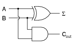


Suppose we wanted to build a device that could add two binary bits together. Such a device is known as a half-adder, and its gate circuit looks like this:

The Σ symbol represents the "sum" output of the half-adder, the sum's least significant bit (LSB). Cout represents the "carry" output of the half-adder, the sum's most significant bit (MSB).
If we were to implement this same function in ladder (relay) logic, it would look like this:
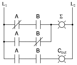
Either circuit is capable of adding two binary digits together. The mathematical "rules" of how to add bits together are intrinsic to the hard-wired logic of the circuits. If we wanted to perform a different arithmetic operation with binary bits, such as multiplication, we would have to construct another circuit. The above circuit designs will only perform one function: add two binary bits together. To make them do something else would take re-wiring, and perhaps different componentry.
In this sense, digital arithmetic circuits aren't much different from analog arithmetic (operational amplifier) circuits: they do exactly what they're wired to do, no more and no less. We are not, however, restricted to designing digital computer circuits in this manner. It is possible to embed the mathematical "rules" for any arithmetic operation in the form of digital data rather than in hard-wired connections between gates. The result is unparalleled flexibility in operation, giving rise to a whole new kind of digital device: the programmable computer.
While this chapter is by no means exhaustive, it provides what I believe is a unique and interesting look at the nature of programmable computer devices, starting with two devices often overlooked in introductory textbooks: look-up table memories and finite-state machines.
Having learned about digital memory devices in the last chapter, we know that it is possible to store binary data within solid-state devices. Those storage "cells" within solid-state memory devices are easily addressed by driving the "address" lines of the device with the proper binary value(s). Suppose we had a ROM memory circuit written, or programmed, with certain data, such that the address lines of the ROM served as inputs and the data lines of the ROM served as outputs, generating the characteristic response of a particular logic function. Theoretically, we could program this ROM chip to emulate whatever logic function we wanted without having to alter any wire connections or gates.
Consider the following example of a 4 x 2 bit ROM memory (a very small memory!) programmed with the functionality of a half adder:
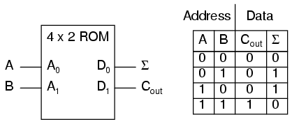
If this ROM has been written with the above data (representing a half-adder's truth table), driving the A and B address inputs will cause the respective memory cells in the ROM chip to be enabled, thus outputting the corresponding data as the Σ (Sum) and Cout bits. Unlike the half-adder circuit built of gates or relays, this device can be set up to perform any logic function at all with two inputs and two outputs, not just the half-adder function. To change the logic function, all we would need to do is write a different table of data to another ROM chip. We could even use an EPROM chip which could be re-written at will, giving the ultimate flexibility in function.
It is vitally important to recognize the significance of this principle as applied to digital circuitry. Whereas the half-adder built from gates or relays processes the input bits to arrive at a specific output, the ROM simply remembers what the outputs should be for any given combination of inputs. This is not much different from the "times tables" memorized in grade school: rather than having to calculate the product of 5 times 6 (5 + 5 + 5 + 5 + 5 + 5 = 30), school-children are taught to remember that 5 x 6 = 30, and then expected to recall this product from memory as needed. Likewise, rather than the logic function depending on the functional arrangement of hard-wired gates or relays (hardware), it depends solely on the data written into the memory (software).
Such a simple application, with definite outputs for every input, is called a look-up table, because the memory device simply "looks up" what the output(s) should to be for any given combination of inputs states.
This application of a memory device to perform logical functions is significant for several reasons:
The usefulness of a look-up table becomes more and more evident with increasing complexity of function. Suppose we wanted to build a 4-bit adder circuit using a ROM. We'd require a ROM with 8 address lines (two 4-bit numbers to be added together), plus 4 data lines (for the signed output):
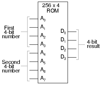
With 256 addressable memory locations in this ROM chip, we would have a fair amount of programming to do, telling it what binary output to generate for each and every combination of binary inputs. We would also run the risk of making a mistake in our programming and have it output an incorrect sum, if we weren't careful. However, the flexibility of being able to configure this function (or any function) through software alone generally outweighs that costs.
Consider some of the advanced functions we could implement with the above "adder." We know that when we add two sets of numbers in 2's complement signed notation, we risk having the answer overflow. For instance, if we try to add 0111 (decimal 7) to 0110 (decimal 6) with only a 4-bit number field, the answer we'll get is 1001 (decimal -7) instead of the correct value, 13 (7 + 6), which cannot be expressed using 4 signed bits. If we wanted to, we could avoid the strange answers given in overflow conditions by programming this look-up table circuit to output something else in conditions where we know overflow will occur (that is, in any case where the real sum would exceed +7 or -8). One alternative might be to program the ROM to output the quantity 0111 (the maximum positive value that can be represented with 4 signed bits), or any other value that we determined to be more appropriate for the application than the typical overflowed "error" value that a regular adder circuit would output. It's all up to the programmer to decide what he or she wants this circuit to do, because we are no longer limited by the constraints of logic gate functions.
The possibilities don't stop at customized logic functions, either. By adding more address lines to the 256 x 4 ROM chip, we can expand the look-up table to include multiple functions:
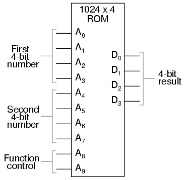
With two more address lines, the ROM chip will have 4 times as many addresses as before (1024 instead of 256). This ROM could be programmed so that when A8 and A9 were both low, the output data represented the sum of the two 4-bit binary numbers input on address lines A0 through A7, just as we had with the previous 256 x 4 ROM circuit. For the addresses A8=1 and A9=0, it could be programmed to output the difference (subtraction) between the first 4-bit binary number (A0 through A3) and the second binary number (A4 through A7). For the addresses A8=0 and A9=1, we could program the ROM to output the difference (subtraction) of the two numbers in reverse order (second - first rather than first - second), and finally, for the addresses A8=1 and A9=1, the ROM could be programmed to compare the two inputs and output an indication of equality or inequality. What we will have then is a device that can perform four different arithmetical operations on 4-bit binary numbers, all by "looking up" the answers programmed into it.
If we had used a ROM chip with more than two additional address lines, we could program it with a wider variety of functions to perform on the two 4-bit inputs. There are a number of operations peculiar to binary data (such as parity check or Exclusive-ORing of bits) that we might find useful to have programmed in such a look-up table.
Devices such as this, which can perform a variety of arithmetical tasks as dictated by a binary input code, are known as Arithmetic Logic Units (ALUs), and they comprise one of the essential components of computer technology. Although modern ALUs are more often constructed from very complex combinational logic (gate) circuits for reasons of speed, it should be comforting to know that the exact same functionality may be duplicated with a "dumb" ROM chip programmed with the appropriate look-up table(s). In fact, this exact approach was used by IBM engineers in 1959 with the development of the IBM 1401 and 1620 computers, which used look-up tables to perform addition, rather than binary adder circuitry. The machine was fondly known as the "CADET," which stood for "Can't Add, Doesn't Even Try."
A very common application for look-up table ROMs is in control systems where a custom mathematical function needs to be represented. Such an application is found in computer-controlled fuel injection systems for automobile engines, where the proper air/fuel mixture ratio for efficient and clean operation changes with several environmental and operational variables. Tests performed on engines in research laboratories determine what these ideal ratios are for varying conditions of engine load, ambient air temperature, and barometric air pressure. The variables are measured with sensor transducers, their analog outputs converted to digital signals with A/D circuitry, and those parallel digital signals used as address inputs to a high-capacity ROM chip programmed to output the optimum digital value for air/fuel ratio for any of these given conditions.
Sometimes, ROMs are used to provide one-dimensional look-up table functions, for "correcting" digitized signal values so that they more accurately represent their real-world significance. An example of such a device is a thermocouple transmitter, which measures the millivoltage signal generated by a junction of dissimilar metals and outputs a signal which is supposed to directly correspond to that junction temperature. Unfortunately, thermocouple junctions do not have perfectly linear temperature/voltage responses, and so the raw voltage signal is not perfectly proportional to temperature. By digitizing the voltage signal (A/D conversion) and sending that digital value to the address of a ROM programmed with the necessary correction values, the ROM's programming could eliminate some of the nonlinearity of the thermocouple's temperature-to-millivoltage relationship, so that the final output of the device would be more accurate. The popular instrumentation term for such a look-up table is a digital characterizer.

Another application for look-up tables is in special code translation. A 128 x 8 ROM, for instance, could be used to translate 7-bit ASCII code to 8-bit EBCDIC code:
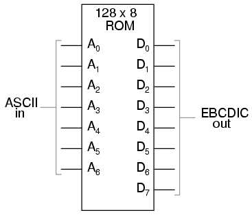
Again, all that is required is for the ROM chip to be properly programmed with the necessary data so that each valid ASCII input will produce a corresponding EBCDIC output code.
Feedback is a fascinating engineering principle. It can turn a rather simple device or process into something substantially more complex. We've seen the effects of feedback intentionally integrated into circuit designs with some rather astounding effects:
In the field of process instrumentation, feedback is used to transform a simple measurement system into something capable of control:
Feedback, both positive and negative, has the tendency to add whole new dynamics to the operation of a device or system. Sometimes, these new dynamics find useful application, while other times they are merely interesting. With look-up tables programmed into memory devices, feedback from the data outputs back to the address inputs creates a whole new type of device: the Finite State Machine, or FSM:
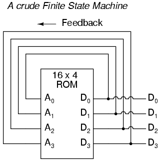
The above circuit illustrates the basic idea: the data stored at each address becomes the next storage location that the ROM gets addressed to. The result is a specific sequence of binary numbers (following the sequence programmed into the ROM) at the output, over time. To avoid signal timing problems, though, we need to connect the data outputs back to the address inputs through a 4-bit D-type flip-flop, so that the sequence takes place step by step to the beat of a controlled clock pulse:
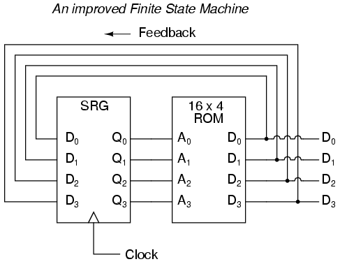
An analogy for the workings of such a device might be an array of post-office boxes, each one with an identifying number on the door (the address), and each one containing a piece of paper with the address of another P.O. box written on it (the data). A person, opening the first P.O. box, would find in it the address of the next P.O. box to open. By storing a particular pattern of addresses in the P.O. boxes, we can dictate the sequence in which each box gets opened, and therefore the sequence of which paper gets read.
Having 16 addressable memory locations in the ROM, this Finite State Machine would have 16 different stable "states" in which it could latch. In each of those states, the identity of the next state would be programmed in to the ROM, awaiting the signal of the next clock pulse to be fed back to the ROM as an address. One useful application of such an FSM would be to generate an arbitrary count sequence, such as Gray Code:
Address  -----> Data          Gray Code count sequence:
0000   -------> 0001                 0   0000
0001   -------> 0011                 1   0001
0010   -------> 0110                 2   0011
0011   -------> 0010                 3   0010
0100   -------> 1100                 4   0110
0101   -------> 0100                 5   0111
0110   -------> 0111                 6   0101
0111   -------> 0101                 7   0100
1000   -------> 0000                 8   1100
1001   -------> 1000                 9   1101
1010   -------> 1011                10   1111
1011   -------> 1001                11   1110
1100   -------> 1101                12   1010
1101   -------> 1111                13   1011
1110   -------> 1010                14   1001
1111   -------> 1110                15   1000
Try to follow the Gray Code count sequence as the FSM would do it: starting at 0000, follow the data stored at that address (0001) to the next address, and so on (0011), and so on (0010), and so on (0110), etc. The result, for the program table shown, is that the sequence of addressing jumps around from address to address in what looks like a haphazard fashion, but when you check each address that is accessed, you will find that it follows the correct order for 4-bit Gray code. When the FSM arrives at its last programmed state (address 1000), the data stored there is 0000, which starts the whole sequence over again at address 0000 in step with the next clock pulse.
We could expand on the capabilities of the above circuit by using a ROM with more address lines, and adding more programming data:
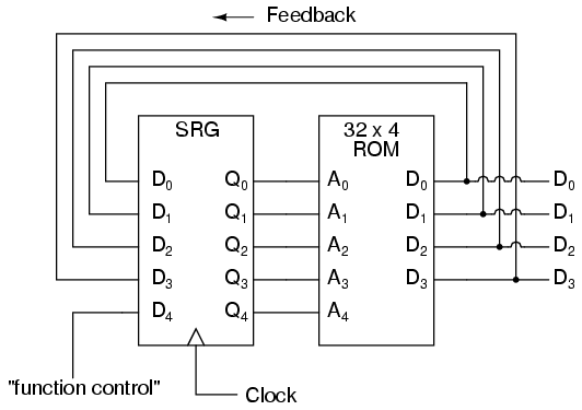
Now, just like the look-up table adder circuit that we turned into an Arithmetic Logic Unit (+, -, x, / functions) by utilizing more address lines as "function control" inputs, this FSM counter can be used to generate more than one count sequence, a different sequence programmed for the four feedback bits (A0 through A3) for each of the two function control line input combinations (A4 = 0 or 1).
Address  -----> Data            Address  -----> Data
00000  -------> 0001            10000  -------> 0001
00001  -------> 0010            10001  -------> 0011
00010  -------> 0011            10010  -------> 0110
00011  -------> 0100            10011  -------> 0010
00100  -------> 0101            10100  -------> 1100
00101  -------> 0110            10101  -------> 0100
00110  -------> 0111            10110  -------> 0111
00111  -------> 1000            10111  -------> 0101
01000  -------> 1001            11000  -------> 0000
01001  -------> 1010            11001  -------> 1000
01010  -------> 1011            11010  -------> 1011
01011  -------> 1100            11011  -------> 1001
01100  -------> 1101            11100  -------> 1101
01101  -------> 1110            11101  -------> 1111
01110  -------> 1111            11110  -------> 1010
01111  -------> 0000            11111  -------> 1110
If A4 is 0, the FSM counts in binary; if A4 is 1, the FSM counts in Gray Code. In either case, the counting sequence is arbitrary: determined by the whim of the programmer. For that matter, the counting sequence doesn't even have to have 16 steps, as the programmer may decide to have the sequence recycle to 0000 at any one of the steps at all. It is a completely flexible counting device, the behavior strictly determined by the software (programming) in the ROM.
We can expand on the capabilities of the FSM even more by utilizing a ROM chip with additional address input and data output lines. Take the following circuit, for example:
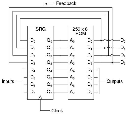
Here, the D0 through D3 data outputs are used exclusively for feedback to the A0 through A3 address lines. Date output lines D4 through D7 can be programmed to output something other than the FSM's "state" value. Being that four data output bits are being fed back to four address bits, this is still a 16-state device. However, having the output data come from other data output lines gives the programmer more freedom to configure functions than before. In other words, this device can do far more than just count! The programmed output of this FSM is dependent not only upon the state of the feedback address lines (A0 through A3), but also the states of the input lines (A4 through A7). The D-type flip/flop's clock signal input does not have to come from a pulse generator, either. To make things more interesting, the flip/flop could be wired up to clock on some external event, so that the FSM goes to the next state only when an input signal tells it to.
Now we have a device that better fulfills the meaning of the word "programmable." The data written to the ROM is a program in the truest sense: the outputs follow a pre-established order based on the inputs to the device and which "step" the device is on in its sequence. This is very close to the operating design of the Turing Machine, a theoretical computing device invented by Alan Turing, mathematically proven to be able to solve any known arithmetic problem, given enough memory capacity.
Early computer science pioneers such as Alan Turing and John Von Neumann postulated that for a computing device to be really useful, it not only had to be able to generate specific outputs as dictated by programmed instructions, but it also had to be able to write data to memory, and be able to act on that data later. Both the program steps and the processed data were to reside in a common memory "pool," thus giving way to the label of the stored-program computer. Turing's theoretical machine utilized a sequential-access tape, which would store data for a control circuit to read, the control circuit re-writing data to the tape and/or moving the tape to a new position to read more data. Modern computers use random-access memory devices instead of sequential-access tapes to accomplish essentially the same thing, except with greater capability.
A helpful illustration is that of early automatic machine tool control technology. Called open-loop, or sometimes just NC (numerical control), these control systems would direct the motion of a machine tool such as a lathe or a mill by following instructions programmed as holes in paper tape. The tape would be run one direction through a "read" mechanism, and the machine would blindly follow the instructions on the tape without regard to any other conditions. While these devices eliminated the burden of having to have a human machinist direct every motion of the machine tool, it was limited in usefulness. Because the machine was blind to the real world, only following the instructions written on the tape, it could not compensate for changing conditions such as expansion of the metal or wear of the mechanisms. Also, the tape programmer had to be acutely aware of the sequence of previous instructions in the machine's program to avoid troublesome circumstances (such as telling the machine tool to move the drill bit laterally while it is still inserted into a hole in the work), since the device had no memory other than the tape itself, which was read-only. Upgrading from a simple tape reader to a Finite State control design gave the device a sort of memory that could be used to keep track of what it had already done (through feedback of some of the data bits to the address bits), so at least the programmer could decide to have the circuit remember "states" that the machine tool could be in (such as "coolant on," or tool position). However, there was still room for improvement.
The ultimate approach is to have the program give instructions which would include the writing of new data to a read/write (RAM) memory, which the program could easily recall and process. This way, the control system could record what it had done, and any sensor-detectable process changes, much in the same way that a human machinist might jot down notes or measurements on a scratch-pad for future reference in his or her work. This is what is referred to as CNC, or Closed-loop Numerical Control.
Engineers and computer scientists looked forward to the possibility of building digital devices that could modify their own programming, much the same as the human brain adapts the strength of inter-neural connections depending on environmental experiences (that is why memory retention improves with repeated study, and behavior is modified through consequential feedback). Only if the computer's program were stored in the same writable memory "pool" as the data would this be practical. It is interesting to note that the notion of a self-modifying program is still considered to be on the cutting edge of computer science. Most computer programming relies on rather fixed sequences of instructions, with a separate field of data being the only information that gets altered.
To facilitate the stored-program approach, we require a device that is much more complex than the simple FSM, although many of the same principles apply. First, we need read/write memory that can be easily accessed: this is easy enough to do. Static or dynamic RAM chips do the job well, and are inexpensive. Secondly, we need some form of logic to process the data stored in memory. Because standard and Boolean arithmetic functions are so useful, we can use an Arithmetic Logic Unit (ALU) such as the look-up table ROM example explored earlier. Finally, we need a device that controls how and where data flows between the memory, the ALU, and the outside world. This so-called Control Unit is the most mysterious piece of the puzzle yet, being comprised of tri-state buffers (to direct data to and from buses) and decoding logic which interprets certain binary codes as instructions to carry out. Sample instructions might be something like: "add the number stored at memory address 0010 with the number stored at memory address 1101," or, "determine the parity of the data in memory address 0111." The choice of which binary codes represent which instructions for the Control Unit to decode is largely arbitrary, just as the choice of which binary codes to use in representing the letters of the alphabet in the ASCII standard was largely arbitrary. ASCII, however, is now an internationally recognized standard, whereas control unit instruction codes are almost always manufacturer-specific.
Putting these components together (read/write memory, ALU, and control unit) results in a digital device that is typically called a processor. If minimal memory is used, and all the necessary components are contained on a single integrated circuit, it is called a microprocessor. When combined with the necessary bus-control support circuitry, it is known as a Central Processing Unit, or CPU.
CPU operation is summed up in the so-called fetch/execute cycle. Fetch means to read an instruction from memory for the Control Unit to decode. A small binary counter in the CPU (known as the program counter or instruction pointer) holds the address value where the next instruction is stored in main memory. The Control Unit sends this binary address value to the main memory's address lines, and the memory's data output is read by the Control Unit to send to another holding register. If the fetched instruction requires reading more data from memory (for example, in adding two numbers together, we have to read both the numbers that are to be added from main memory or from some other source), the Control Unit appropriately addresses the location of the requested data and directs the data output to ALU registers. Next, the Control Unit would execute the instruction by signaling the ALU to do whatever was requested with the two numbers, and direct the result to another register called the accumulator. The instruction has now been "fetched" and "executed," so the Control Unit now increments the program counter to step the next instruction, and the cycle repeats itself.
        Microprocessor (CPU)

--------------------------------------
|       ** Program counter **        |
|  (increments address value sent to |
|  external memory chip(s) to fetch  |==========> Address bus
|  the next instruction)             |          (to RAM memory)
--------------------------------------
|        ** Control Unit **          |<=========> Control Bus
|  (decodes instructions read from   | (to all devices sharing
|  program in memory, enables flow   | address and/or data busses;
|  of data to and from ALU, internal | arbitrates all bus communi-
|  registers, and external devices)  | cations)
--------------------------------------
| ** Arithmetic Logic Unit (ALU) **  |
|    (performs all mathematical      |
|     calculations and Boolean       |
|     functions)                     |
--------------------------------------
|          ** Registers **           |
|    (small read/write memories for  |<=========> Data Bus
|     holding instruction codes,     | (from RAM memory and other
|     error codes, ALU data, etc;    |  external devices)
|     includes the "accumulator")    |
--------------------------------------
As one might guess, carrying out even simple instructions is a tedious process. Several steps are necessary for the Control Unit to complete the simplest of mathematical procedures. This is especially true for arithmetic procedures such as exponents, which involve repeated executions ("iterations") of simpler functions. Just imagine the sheer quantity of steps necessary within the CPU to update the bits of information for the graphic display on a flight simulator game! The only thing which makes such a tedious process practical is the fact that microprocessor circuits are able to repeat the fetch/execute cycle with great speed.
In some microprocessor designs, there are minimal programs stored within a special ROM memory internal to the device (called microcode) which handle all the sub-steps necessary to carry out more complex math operations. This way, only a single instruction has to be read from the program RAM to do the task, and the programmer doesn't have to deal with trying to tell the microprocessor how to do every minute step. In essence, it's a processor inside of a processor; a program running inside of a program.
The "vocabulary" of instructions which any particular microprocessor chip possesses is specific to that model of chip. An Intel 80386, for example, uses a completely different set of binary codes than a Motorola 68020, for designating equivalent functions. Unfortunately, there are no standards in place for microprocessor instructions. This makes programming at the very lowest level very confusing and specialized.
When a human programmer develops a set of instructions to directly tell a microprocessor how to do something (like automatically control the fuel injection rate to an engine), they're programming in the CPU's own "language." This language, which consists of the very same binary codes which the Control Unit inside the CPU chip decodes to perform tasks, is often referred to as machine language. While machine language software can be "worded" in binary notation, it is often written in hexadecimal form, because it is easier for human beings to work with. For example, I'll present just a few of the common instruction codes for the Intel 8080 micro-processor chip:
Hexadecimal    Binary              Instruction description
-----------   --------   -----------------------------------------
|   7B        01111011   Move contents of register A to register E
|
|   87        10000111   Add contents of register A to register D
|
|   1C        00011100   Increment the contents of register E by 1
|
|   D3        11010011   Output byte of data to data bus
Even with hexadecimal notation, these instructions can be easily confused and forgotten. For this purpose, another aid for programmers exists called assembly language. With assembly language, two to four letter mnemonic words are used in place of the actual hex or binary code for describing program steps. For example, the instruction 7B for the Intel 8080 would be "MOV A,E" in assembly language. The mnemonics, of course, are useless to the microprocessor, which can only understand binary codes, but it is an expedient way for programmers to manage the writing of their programs on paper or text editor (word processor). There are even programs written for computers called assemblers which understand these mnemonics, translating them to the appropriate binary codes for a specified target microprocessor, so that the programmer can write a program in the computer's native language without ever having to deal with strange hex or tedious binary code notation.
Once a program is developed by a person, it must be written into memory before a microprocessor can execute it. If the program is to be stored in ROM (which some are), this can be done with a special machine called a ROM programmer, or (if you're masochistic), by plugging the ROM chip into a breadboard, powering it up with the appropriate voltages, and writing data by making the right wire connections to the address and data lines, one at a time, for each instruction. If the program is to be stored in volatile memory, such as the operating computer's RAM memory, there may be a way to type it in by hand through that computer's keyboard (some computers have a mini-program stored in ROM which tells the microprocessor how to accept keystrokes from a keyboard and store them as commands in RAM), even if it is too dumb to do anything else. Many "hobby" computer kits work like this. If the computer to be programmed is a fully-functional personal computer with an operating system, disk drives, and the whole works, you can simply command the assembler to store your finished program onto a disk for later retrieval. To "run" your program, you would simply type your program's filename at the prompt, press the Enter key, and the microprocessor's Program Counter register would be set to point to the location ("address") on the disk where the first instruction is stored, and your program would run from there.
Although programming in machine language or assembly language makes for fast and highly efficient programs, it takes a lot of time and skill to do so for anything but the simplest tasks, because each machine language instruction is so crude. The answer to this is to develop ways for programmers to write in "high level" languages, which can more efficiently express human thought. Instead of typing in dozens of cryptic assembly language codes, a programmer writing in a high-level language would be able to write something like this . . .
Print "Hello, world!"
. . . and expect the computer to print "Hello, world!" with no further instruction on how to do so. This is a great idea, but how does a microprocessor understand such "human" thinking when its vocabulary is so limited?
The answer comes in two different forms: interpretation, or compilation. Just like two people speaking different languages, there has to be some way to transcend the language barrier in order for them to converse. A translator is needed to translate each person's words to the other person's language, one way at a time. For the microprocessor, this means another program, written by another programmer in machine language, which recognizes the ASCII character patterns of high-level commands such as Print (P-r-i-n-t) and can translate them into the necessary bite-size steps that the microprocessor can directly understand. If this translation is done during program execution, just like a translator intervening between two people in a live conversation, it is called "interpretation." On the other hand, if the entire program is translated to machine language in one fell swoop, like a translator recording a monologue on paper and then translating all the words at one sitting into a written document in the other language, the process is called "compilation."
Interpretation is simple, but makes for a slow-running program because the microprocessor has to continually translate the program between steps, and that takes time. Compilation takes time initially to translate the whole program into machine code, but the resulting machine code needs no translation after that and runs faster as a consequence. Programming languages such as BASIC and FORTH are interpreted. Languages such as C, C++, FORTRAN, and PASCAL are compiled. Compiled languages are generally considered to be the languages of choice for professional programmers, because of the efficiency of the final product.
Naturally, because machine language vocabularies vary widely from microprocessor to microprocessor, and since high-level languages are designed to be as universal as possible, the interpreting and compiling programs necessary for language translation must be microprocessor-specific. Development of these interpreters and compilers is a most impressive feat: the people who make these programs most definitely earn their keep, especially when you consider the work they must do to keep their software product current with the rapidly-changing microprocessor models appearing on the market!
To mitigate this difficulty, the trend-setting manufacturers of microprocessor chips (most notably, Intel and Motorola) try to design their new products to be backwardly compatible with their older products. For example, the entire instruction set for the Intel 80386 chip is contained within the latest Pentium IV chips, although the Pentium chips have additional instructions that the 80386 chips lack. What this means is that machine-language programs (compilers, too) written for 80386 computers will run on the latest and greatest Intel Pentium IV CPU, but machine-language programs written specifically to take advantage of the Pentium's larger instruction set will not run on an 80386, because the older CPU simply doesn't have some of those instructions in its vocabulary: the Control Unit inside the 80386 cannot decode them.
Building on this theme, most compilers have settings that allow the programmer to select which CPU type he or she wants to compile machine-language code for. If they select the 80386 setting, the compiler will perform the translation using only instructions known to the 80386 chip; if they select the Pentium setting, the compiler is free to make use of all instructions known to Pentiums. This is analogous to telling a translator what minimum reading level their audience will be: a document translated for a child will be understandable to an adult, but a document translated for an adult may very well be gibberish to a child.
Lessons In Electric Circuits copyright (C) 2000-2007 Tony R. Kuphaldt, under the terms and conditions of the Design Science License.


