CSCI 2150
Spring 2001 Test 2 -- Answers
The following is the answers to the Spring 2001 CSCI 2150
Test 2. In some cases, where the HTML does not prohibit it,
I've elaborated on the process to get to the answers.
- Which of the following is an invalid state of an S-R flip-flop?
Answer: A -- ^S and ^R cannot be zero at the same time. This is
like setting and resetting an output at the same time.
- True or false: The D flip-flop has no invalid states.
Answer: True -- This question is probably worded incorrectly. It should
probably say, "The D flip-flop with only CLK and D inputs has
no invalid states." In this case, there are no states that
cause problems with the outputs.
- If a D flip-flop has the inputs ^S=1, ^R=0, D=1, & CLK=0, what
is the output Q?
Answer: Q=0 -- The ^R=0 overrides any of the other inputs forcing
Q to equal zero.
- The D flip-flop circuit below is one of the special applications
we studied in class. Even if you don't remember the circuit, you
should still be able to draw the output based on the system clock
input. Assume flip-flop captures D on the clock's rising edge.
Answer: The answer is in red in the figure below.

- What is the minimum number of D flip-flops you will need to
represent the states of a state diagram with 24 states?
Answer: 5 -- If you number the states, you should come up with a list
going from 0 to 23. And what is 23 in binary? 10111. Since it
takes 5 bits to represent 23, then five flip-flops are going to
be required to remember 24 distinct states. Another way of looking
at it is that 1 flip-flop can remember 21=2 states,
2 flip-flops can remember 22=4 states,
3 flip-flops can remember 23=8 states,
4 flip-flops can remember 24=16 states, and
5 flip-flops can remember 25=32 states. 1, 2, 3, and 4
are not enough. Five is the first value that has more than
25 possible states.
- Create the next state truth table and the output truth table
from the state diagram below. (The diagram is omitted from this answer
key. You can see it from the PDF file of the
test.) Make sure you label the bits of your states using the
state numbers from the diagram.
Answer:
| Next State Table |
|
Current State
|
D
|
Next State
|
| S1 |
S0 |
S1' |
S0' |
| 0 | 0 | 0 | 0 | 1 |
| 0 | 0 | 1 | 1 | 1 |
| 0 | 1 | 0 | 1 | 1 |
| 0 | 1 | 1 | 1 | 0 |
| 1 | 0 | 0 | 1 | 1 |
| 1 | 0 | 1 | 0 | 1 |
| 1 | 1 | 0 | 0 | 0 |
| 1 | 1 | 1 | 1 | 0 |
|
| Output Table |
|
Current State
|
Output
|
| S1 |
S0 |
| 0 | 0 | 1 |
| 0 | 1 | 0 |
| 1 | 0 | 1 |
| 1 | 1 | 0 |
|
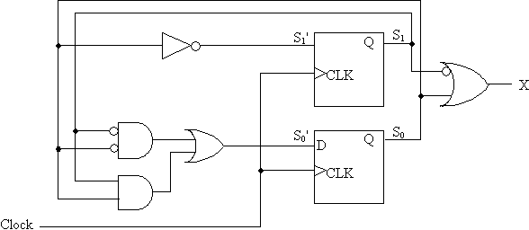
- The three Boolean expressions below represent the next
state bits (S0' and S1') and the output bit (X) based on the
current state (S0 and S1). Draw the logic circuit for the
state machine including the flip-flops and output circuitry.
S0' = (^S0 ^S1) + (S0 S1)
S1' = ^S0
X = S0 + ^S1
Answer:

- Connect input A of the XOR gate shown to the right so as
to invert input B at the XOR gate's output.
Answer: Connect A to a logic 1 value.
- A connection between a row and a column in a
PAL array is made by:
- Blowing a fusible link
- Leaving a fusible link
- Wiring an input variable to the input line
- Wiring an input variable to the product term line
Answer: B
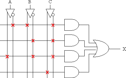
- Using the shorthand notation, set the PAL diagram
below to represent the boolean expression
X = (^A B ^C) + (^B ^C) + (A ^B ^C) + C.
Answer:

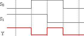
- For the multiplexer/selector shown to the right, sketch the output
waveform Y for the inputs S0 and S1 shown below?
Answer:

- The bit capacity (i.e., the total number of flip-flops) in a RAM
with 12 address lines and 8 bits stored at each address is:
Answer: a.) 32,768 -- The number of flip-flops equals the number of bits
of data times the number of address locations. The number of address
locations is 2number of address lines. Therefore, the
answer is 8 x 212 = 8 x 4096 = 32,768.
- Of the bus control lines, the write line goes
low when:
- Data is passing from memory to processor
- The bus is idle
- Data is passing from processor to memory
- Cannot tell without read line value
Answer: C
- Circle all that apply. A storage cell in a DRAM:
- is volatile
- is a capacitor
- needs to be refreshed regularly
- is smaller than a cell in an SRAM
Answer: a, b, c, and d
- Circle all the memory types below that are
non-volatile.
- SRAM
- Flash RAM
- Custom-masked ROM
- EEPROM
- OTPROM
- DRAM
Answer: b, c, d, and e
- Circle all the memory types below that can
be written to multiple times.
- Battery-backed SRAM
- Flash RAM
- Custom-masked ROM
- EEPROM
- OTPROM
- EPROM
Answer: a, b, d, and f
- True or False: One memory block can have a low address of
340016 and a high address of 3FFF16?
Answer: False -- 340016 = 0011 0100 0000 00002 and
3FFF16 = 0011 1111 1111 11112. Since the low address
has all of its least significant 0's from position 0 to position 9, then positions
10 through 15 must be the same for both addresses. They are not. Position
11 is a 0 in the low address and a 1 in the high address. No chip select can
be made for this.
- What is the high address IN HEX for
a 1K ROM with a low address of 380016?
Answer: 3BFF16 -- A ROM with an address space of 1K needs 10 address lines.
Therefore, the low address must have positions 0 through 9 equal to a zero
and the high address must have positions 0 through 9 equal to a one. All
other bit positions must remain the same. Therefore, since 380016 =
0011 1000 0000 00002, then switching positions
0 through 9 gives us 0011 1011 1111 1111 = 3BFF16.
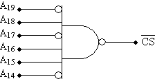
- Design the chip select (w/logic gates) for a 16K
RAM placed in a 1MEG memory space with a low address of
5800016. Label all address lines
used for chip select.
Answer:

Created by David Tarnoff for use by his sections of CSCI 2150.

