Answers Database
M1.3/FPGA Express: M1 Constraints, LogiBLOX, and modules within FPGA Express

Record #2735
Product Family: Software
Product Line: Synopsys
Problem Title:
M1.3/FPGA Express: M1 Constraints, LogiBLOX, and modules within FPGA
Express
Problem Description:
Keywords: constraints, cst, FPGA Express, FPGA, Express, timing, location,
LogiBLOX, RAM, FFS, FF
Urgency: standard
General Description:
This solution is an overview of using M1 constraints with FPGA Express as the
top-level design tool. Constraints that FPGA Express can directly apply will
be documented. Information on how to reference instance names in XNF files
from FPGA Express will be documented; when constraints are needed that FPGA
Express cannot apply, a UCF file referencing instance names in the XNF file
will be made. Similarly, information on how to reference the instances inside
LogiBLOX RAM/ROM modules will also be provided for creating UCF constraints.
Solution 1:
What are M1 logical constraints?
In the M1 design flow, constraints or attributes that can be applied within a
schematic, netlist, and/or UCF file are known as logical constraints.
Logical constraints restrict the placement or timing of logic in an FPGA or
CPLD design. In order to use a logical constraint correctly, the "instance"
name of logic in a design must be used. Instance names are XNF SYM record
names, XNF SIG record names, XNF net names, and EXT record names.
For examples of reading these instance names out of a XNF file from FPGA
Express, refer to Figure 1.
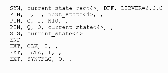
Figure 1- XNF Example
In Figure 1, the SYM record name can be referenced by a logical constraint
by using the instance name "current_state_reg<4>". A net called "N10" or
"current_state<4>" can also be used in a logical constraint. EXT records
correspond to pins used on a package. The EXT records named "CLK", "DATA"
and "SYNCFLG" can be locked to specific pins.
For more information on M1 constraints, refer to Chapter 13 of the Libraries
Guide.
Solution 2:
Which constraints can be applied by the FPGA Express GUI?
After a design has been "implemented" in FPGA Express, M1 constraints can be
applied to a design through three spreadsheets in the "Implementation"
window. The "Implementation" window is selected by double-clicking on the
particular implementation. See Figures 2 and 3.
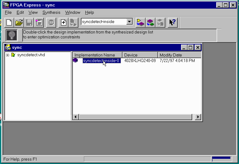
Figure 2- Implemented Design
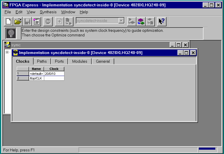
Figure 3- Constraints Spreadsheet
The Implementation window shown in Figure 3 has three different spreadsheets
where M1 constraints can be applied: clock, paths, and ports. The "clock"
spreadsheet allows the user to specify overall speeds for the clocks in a
design. The "paths" spreadsheet allows the user more precise control of
point-to-point timing in a design. The "ports" spreadsheet allows OFFSETS,
pullups/pulldowns, and pin locations to be specified in a design. In general,
if FPGA Express can synthesize it, FPGA Express can apply a constraint to it.
The constraints specified in the Implementation window are translated into
FROM:TO timespecs and placed in the XNF file Express outputs.
Currently, Express can not apply all M1 constraints to a netlist. With the
exception of pin locations, FPGA Express cannot apply area constraints.
FPGA Express timing constraints are limited to PADS, FFS, and LATCHES.
Except LOC and slew rates, most attributes in the M1 flow cannot be applied
by FPGA Express. FPGA Express can create its own timegroups by grouping
logic with common clocks and clock enables. However, this type of grouping
may not be appropriate for the timing of a design in some cases. When the const
raints out of the Express tool are lacking or inappropriate, a UCF file
can be used for specifying logical constraints by referencing the instance
names in the XNF file or LogiBLOX RAM/ROM modules.
Solution 3:
Instance names for LogiBLOX RAM/ROM in the FPGA Express/M1.3 Design Flow
In the M1.3 FPGA Express methodology, whenever large blocks of RAM/ROM are
needed, LogiBLOX RAM/ROM modules are instantiated in the HDL code. With
LogiBLOX RAM/ROM modules instantiated in the HDL code, timing and/or
placement constraints on these RAM/ROM modules and the RAM/ROM primitives
that comprise these modules are specified in a .ucf file. To create timing
and/or placement constraints for RAM/ROM LogiBLOX modules, knowledge of how
many primitives will be used and how the primitives inside the RAM/ROM
LogiBLOX modules are named is needed.
How many primitives are inside a LogiBLOX RAM/ROM module?
When a RAM/ROM is specified with LogiBLOX, the RAM/ROM depth and width are
specified. If the RAM/ROM depth is divisible by 32, then 32x1 primitives are
used. If the RAM/ROM depth is not divisible by 32, then 16x1 primitives are
used instead. In the case ofdual-port RAM’s, 16x1 primitives are always used.
Based on whether 32x1 or 16x1 primitives are used, the number of RAM/ROM
can be calculated.
For example, if a RAM48x4 was required for a design, RAM16x1 primitives would
be used. Based on the width, there would be four banks of RAM16x1's. Based
on the depth, each bank would have three RAM16x1’s.
How are the RAM primitives inside LogiBLOX RAM/ROM modules named?
Using the example of a RAM48x4, the RAM primitives inside the LogiBLOX would
be named as follows:
MEM0_0 MEM1_0 MEM2_0 MEM3_0
MEM0_1 MEM1_1 MEM2_1 MEM3_1
MEM0_2 MEM1_2 MEM2_2 MEM3_2
Each primitive in a LogiBLOX RAM/ROM module has a instance name of MEMx_y,
where "y" represents the primitive position in the bank of memory, and where
"x" represents the bit position of the RAM/ROM output.
Solution 4:
Reading instance names from an Express created XNF file for UCF constraints
In M1, constraints are applied by referencing instance names in the XNF file.
Instance names for logic in a design can be found by reading the XNF file.
Refer to XNF syntax in Figure 1 for the examples in this section.
A TNM constraint can be applied to a FF by using the instance name from
the XNF file. Similarly, a LOC/RLOC can beapplied:
INST "current_state_reg<4>" TNM=group1;
INST "current_state_reg<4>" LOC=CLB_R5C5;
By attaching a TNM to this flip-flop instance name, this flip-flop can be
referenced in a FROM:TO timing specification. Any symbol that can have a M1
constraint applied is referenced by using the string following the keyword:
SYM.
A pin on a device may be locked to a package specific position by
referencing the EXT record name and adding the .PAD string:
INST "DATA.PAD" LOC=P124;
An attribute which can be placed on a net, like KEEP or TNM, can be
referenced by referencing the netname on the PIN record, or SIG record:
NET "current_state<4>" KEEP;
NET "current_state<4>" TNM=group2;
A final note on referencing instance names from a XNF file: match the case.
M1 is case-sensitive. If the case of names in the XNF file is not followed
exactly, the M1 implementation software may not be able to find (or may
incorrectly find) an instance name for a constraint.
Solution 5:
Referencing LogiBLOX modules/components/primitives in the FPGA Express Flow
Note: This final section is written in terms of the Verilog example, using
the files provided in Figures 4 through 7. This section also applies to the
VHDL example in Figures 8 through 10. For information on compiling these
examples, see (Xilinx Solution 2738).
LogiBLOX RAM/ROM modules in the M1 FPGA Express flow are constrained via a
.ucf file. LogiBLOX RAM/ROM modules instantiated in the HDL code can be
referenced by the complete hierarchical instance name. If a LogiBLOX RAM/ROM
module is at the top-level of the HDL code, then the instance name of the
LogiBLOX RAM/ROM module is just the instantiated instance name. In the case
of a LogiBLOX RAM/ROM that is instantiated within the hierarchy of the
design, the instance name of the LogiBLOX RAM/ROM module is the full
hierarchical path down to the LogiBLOX RAM/ROM. The hierarchy level names
are listed from the top level down and are separated by a "_". In the
Verilog example, the RAM32X1S is named "memory". "memory" is instantiated in
Verilog module "inside" with an instance name "U1". "inside" is instantiated
in the top-level module "test" with an instance name "U0". Therefore, the
RAM32X1S can be referenced in a .ucf file as "U0_U1". For example, to attach
a TNM to this block of RAM, the following line could be used in the .ucf file:
INST "U0_U1" TNM=block1;
Since U0_U1 is composed of two RAM primitives, a timegroup called "block1"
would be created; the "block1" TNM could be used throughout the .ucf file as
a timespec end/start point, and/or U0_U1 could have a LOC area constraint
applied to it. If the RAM32X1S has been instantiated in the top-level file,
and the instance name used in the instantiation was "U1", then this block of
RAM could just be referenced by "U1".
Sometimes it will be necessary to apply constraints to the primitives that
compose the LogiBLOX RAM/ROM module. For example, if you choose a
floorplanning strategy to implement your design, it may be necessary to
apply LOC constraints to one or more primitives inside a LogiBLOX RAM/ROM
module. Consider the RAM32X2S example above, suppose that the each of the
RAM primitives had to be constrained to a particular CLB location. Based on
the rules for determining the MEMx_y instance names, using the example from
above, each of RAM primitives could be referenced by concatenating the
full-hierarchical name to each of the MEMx_y names. The RAM32x2S created by
LogiBLOX would have primitives named MEM0_0 and MEM1_0, so CLB constraints
in a .ucf file for each of these two items would be:
INST "U0_U1/MEM0_0" LOC=CLB_R10C10;
INST "U0_U1/MEM0_1" LOC=CLB_R11C11;
Solution 6:
Verilog Example files:
test.v:
module test(DATA,DATAOUT,ADDR,C,ENB);
input [1:0] DATA;
output [1:0] DATAOUT;
input [4:0] ADDR;
input C;
input ENB;
wire [1:0] dataoutreg;
reg [1:0] datareg;
reg [1:0] DATAOUT;
reg [4:0] addrreg;
inside U0
(.MDATA(datareg),.MDATAOUT(dataoutreg),.MADDR(addrreg),.C(C),.WE(ENB));
always@(posedge C)
datareg = DATA;
always@(posedge C)
DATAOUT = dataoutreg;
always@(posedge C)
addrreg = ADDR;
endmodule
inside.v:
module inside(MDATA,MDATAOUT,MADDR,C,WE);
input [1:0] MDATA;
output [1:0] MDATAOUT;
input [4:0] MADDR;
input C;
input WE;
memory U1
( .A(MADDR),
.DO(MDATAOUT),
.DI(MDATA),
.WR_EN(WE),
.WR_CLK(C));
endmodule
memory.v:
module memory(A,DO,DI,WR_EN,WR_CLK);
input A;
output DO;
input DI;
input WR_EN;
input WR_CLK;
endmodule
test.ucf:
INST U0_U1 TNM = usermem;
TIMESPEC TS_6= FROM : FFS :TO: usermem: 50;
INST U0_U1/mem0_0 LOC=CLB_R7C2;
VHDL Example files:
test.vhd:
library IEEE;
use IEEE.STD_LOGIC_1164.all;
use IEEE.STD_LOGIC_UNSIGNED.all;
entity test is
port( DATA: in STD_LOGIC_VECTOR(1 downto 0);
DATAOUT: out STD_LOGIC_VECTOR(1 downto 0);
ADDR: in STD_LOGIC_VECTOR(4 downto 0);
C, ENB: in STD_LOGIC);
end test;
architecture details of test is
signal dataoutreg,datareg: STD_LOGIC_VECTOR(1 downto 0);
signal addrreg: STD_LOGIC_VECTOR(4 downto 0);
component inside
port( MDATA: in STD_LOGIC_VECTOR(1 downto 0);
MDATAOUT: out STD_LOGIC_VECTOR(1 downto 0);
MADDR: in STD_LOGIC_VECTOR(4 downto 0);
C,WE: in STD_LOGIC);
end component;
begin
U0: inside port
map(MDATA=>datareg.,MDATAOUT=>dataoutreg.,MADDR=>addrreg,C=>C,WE=>ENB);
process( C )
begin
if(C’event and C=’1’) then
datareg <= DATA;
end if;
end process;
process( C )
begin
if(C’event and C=’1’) then
DATAOUT <= dataoutreg;
end if;
end process;
process( C )
begin
if(C’event and C=’1’) then
addrreg <= ADDR;
end if;
end process;
end details;
inside.vhd:
entity inside is
port( MDATA: in STD_LOGIC_VECTOR(1 downto 0);
MDATAOUT: out STD_LOGIC_VECTOR(1 downto 0);
MADDR: in STD_LOGIC_VECTOR(4 downto 0);
C,WE: in STD_LOGIC);
end inside;
architecture details of inside is
component memory
port( A: in STD_LOGIC_VECTOR(4 downto 0);
DO: out STD_LOGIC_VECTOR(1 downto 0);
DI: in STD_LOGIC_VECTOR(1 downto 0);
WR_EN,WR_CLK: in STD_LOGIC);
end component;
begin
U1: memory port map(A=>MADDR,DO=>MDATAOUT,DI=>MDATA,WR_EN=>WE,WR_CLK=>C);
end details;
test.ucf:
INST U0_U1 TNM = usermem;
TIMESPEC TS_6= FROM : FFS :TO: usermem: 50;
INST U0_U1/mem0_0 LOC=CLB_R7C2;
Solution 7:
Applying M1 Constraints to a FPGA Express Module in a Foundation Schematic
FPGA Express v1.2 can be used as a module generator for Foundation. It is
possible to create a design in FPGA Express and export this design as a XNF,
which can be placed in a Foudnation schematic. Please consult the application
note "Modular Design with M1.3 and FPGA Express v1.2" for more details on
creating a module/macro. And like any macro in a Foudnation schematic, it is
possible to apply constraints on the logic of that macro.
-Applying Timing consraints relative to the FPGA Express module only
As an option, FPGA Express can generate timespecs in the XNF files it creates.
If an XNF file form FPGA Express will be used as a macro in a Foundation schemat
ic, these timespecs will only apply to the logic within the module.
FPGA Express creates timegroups by applying TNMs directly to logic in the XNF
file from FPGA Express. Since these TNMs are applied directly to instances,
unless a timespec uses a group name like PADS, LATCHES, RAMS or FFS, the
timespec within the macro will only apply to the macro. Before using the
timing constraints from FPGA Express, a user should check the XNF file for
these group names, since these group names could result in the timespec being
applied to more than just the macro logic.
-Applying M1.3 constraints between logic in a FPGA Express macro and a
Foundation schematic
If a Foundation schematic is used as the top-level in a design, it is
possible to apply consraints on logic inside of a macro, and/or apply
constraints between logic in the schematic and the logic inside the macro.
Only constraints that can be applied as schematic attributes to symbols can
be applied to FPGA Express macros symbols in a Foundation schematic, like
TNM or HBLKNM. See Chapter 13 of the Libraries Guide for more information
on M1 constraints. Constraints applied to a FPGA Express macro symbol will
descend through the macro and apply to its related logic. If you are trying
to apply TNMs to logic in a FPGA Express macro, include a group qualifier
like FFS, PADS, LATCHES or RAMS. This will insure that the TNM gets applied
to the correct logic type.
In the figure below, a symbol called U1 with an applied TNM is shown. Along
with the symbol, the Foundation 'Symbol Properties' window opened on the U1
symbol shows that a TNM with a FFS qualifier is applied to the U1 symbol:
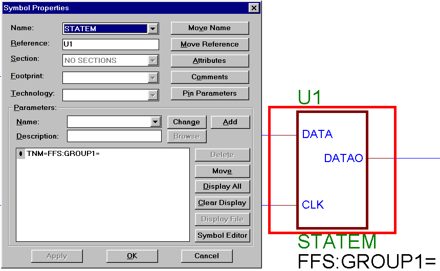
TNM attribute applied to FPGA Express Macro Symbol
End of Record #2735
| For the latest news, design tips, and patch information on the Xilinx design environment, check out the Xilinx Expert Journals! |