Answers Database
M1.3/FPGA Express v1.2: Modular (Black-Box) Instantiation in Express

Record #2738
Product Family: Software
Product Line: Synopsys
Problem Title:
M1.3/FPGA Express v1.2: Modular (Black-Box) Instantiation in Express
Problem Description:
Keywords: instantiate, FPGA Express, VHDL, Verilog, module, modular,
black-box, LogiBLOX, LogiCORE, XNF
Urgency: Standard
General Description:
Instantiation of an XNF netlist, a LogiBLOX .ngo file, and/or LogiCORE in HDL
code is known as modular design. This is also referred to as black-box
instantiation. Modular design with FPGA Express and M1.3 allows HDL code to
be merged with netlists or Intellectual Property modules that have already
been optimized. Modular design methodology requires that a place-holder be
written into the HDL to be compiled by FPGA Express. This place-holder is
used to merge the XNF netlist, LogiBLOX .ngo file, or LogiCORE by NGDBUILD.
Examples of this type of flow are instantiating an XNF from the DSP Core
Generator, instantiating LogiBLOX RAM/ROM, and/or instantiating a LogiCORE
like the PCI Core.
For modular design with FPGA Express, regardless of the type of module (XNF,
LogiBLOX, LogiCORE), there are two methodologies: one for VHDL and one for
Verilog. Both VHDL and Verilog examples will be presented in this solution
record. The examples use LogiBLOX RAM, but the procedure is applicable for
all types of module instantiation. Differences between using XNF, LogiBLOX,
and LogiCORE will be noted in the procedures when necessary.
Solution 1:
LogiBLOX RAM Modular Design Methodlogy using VHDL, FPGA Express v1.2, & M1.3
1. Using LogiBLOX, create a RAM module. When setting up LogiBLOX, in the
"Setup" window, set the vendor to "Synopsys" and the Bus Notation as "B<I>",
as shown in Figure 1.
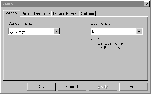
Figure 1- LogiBLOX Vendor Setup
In this example, a RAM48X4S is created. Under the "Options" window in the
"Setup" window, select "VHDL template" and "NGO file", as shown in Figure 2.
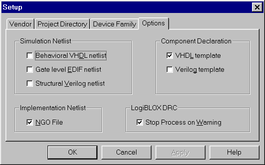
Figure 2- LogiBLOX Options Setup
Next, define the type of LogiBLOX module and its attributes. The Module Name
specified for the LogiBLOX module will be used as the name of the
instantiation in the VHDL code.
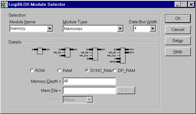
Figure 3- LogiBLOX Module Selector GUI
When the OK button is selected, the LogiBLOX module will be created. This
process will create a number of files, including an .ngo file, which will be
the file merged by ngdbuild, and a .vhi file, which will be used as an instantia
tion reference.
2.Using the .vhi file as a reference, write your VHDL code to instantiate
the LogiBLOX RAM module.
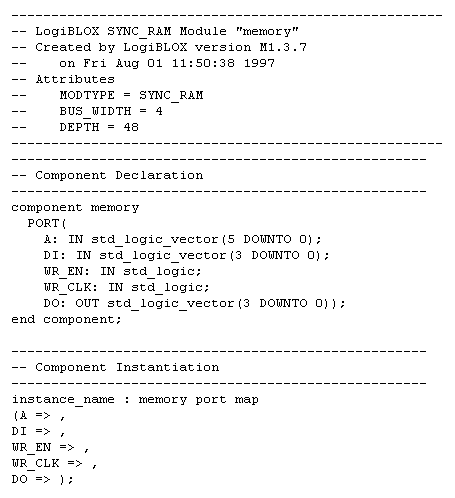
Figure 4- VHI file created by LogiBLOX
The component name is the name given to the LogiBLOX module in the GUI.
The port names are the names provided in the .vhi file.
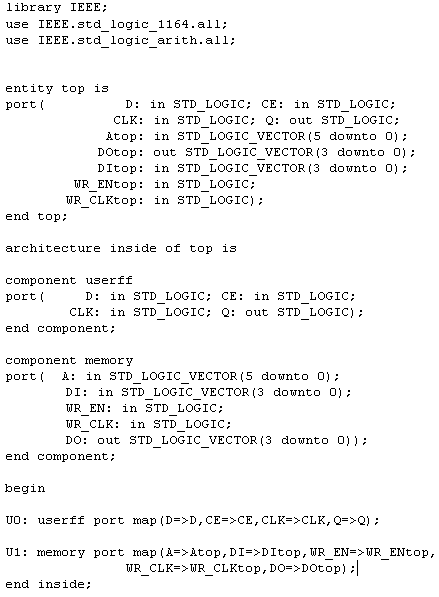
Figure 5- VHDL file with LogiBLOX instantiation
3.At this point, you have a .ngo file from LogiBLOX, and one or more VHDL
files with the .ngo file instantiated. In this example, there is only one
instantiation, but multiple calls to the same module may be done. Read,
analyze, and then implement the design in FPGA Express.
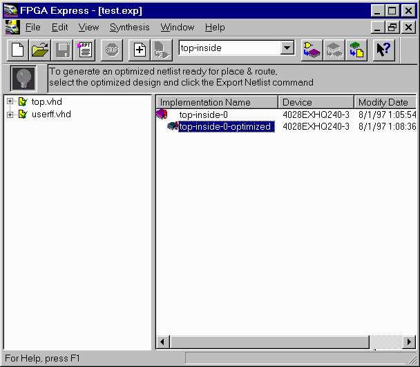
Figure 6- Design Implemented within FPGA Express
4.After implementing the design, select the implementation window and select
"modules". The instantiated LogiBLOX module will show up as "UNLINKED". Preserve
all instantiated LogiBLOX modules.
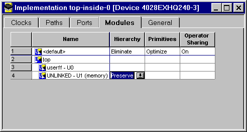
Figure 7- Unlinked LogiBLOX module set to "Preserve"
5. Set all consraints for the rest of the design.
6. Optimize the design.
7.Write out the XNF file. Express will not write out a XNF file for the
instantiated LogiBLOX component.
8.Take the XNF file written by Express and the .ngo file written by LogiBLOX
and process the design through the M1.3 Core Technology software.
Solution 2:
LogiBLOX RAM Modular Design Methodology using Verilog, FPGA Express v1.2, & M1.3
1.Using LogiBLOX, create a RAM module. When setting up LogiBLOX, in the
"Setup" window, set the vendor to "Synopsys" and the Bus Notation as "B<I>",
as shown in Figure 8.
Figure 8- LogiBLOX Vendor setup
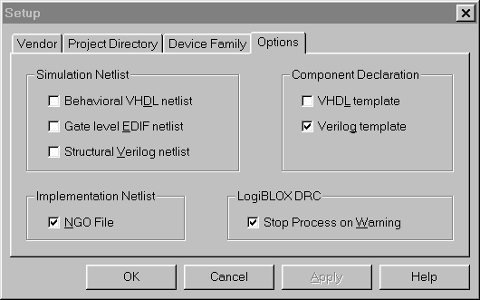
Figure 9- LogiBLOX Options setup
In this example, a RAM48X4S is created. Under the "Options" window in the
"Setup" window, select "Verilog template" and "NGO file", as shown in Figure 10.
Figure 10- LogiBLOX Module Selector GUI
When the OK button is selected, the LogiBLOX module will be created. This
process will create a number of files, including an .ngo file, which will be
the file merged by ngdbuild, and a .vei file, which will be used as an
instantiation reference.
2.Using the .vei file as a reference, write your Verilog code to instantiate
the LogiBLOX RAM module.
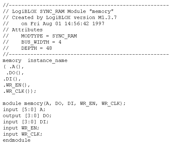
Figure 11- VEI file created by LogiBLOX
The component name is the name given to the LogiBLOX module in the GUI. The
port names are the names provided in the .vei file.
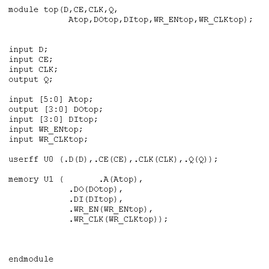
Figure 12- Verilog file with LogiBLOX instantiation
3.At this point, you have a .ngo file from LogiBLOX, and one or more Verilog
files with the .ngo file instantiated. In this example, there is only one
instantiation, but multiple calls to the same module may be done. Read,
analyze, and then implement the design in FPGA Express.
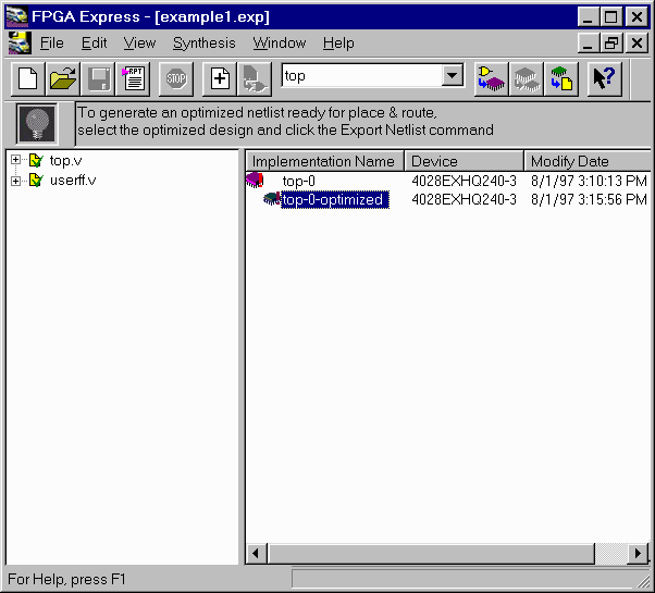
Figure 13- Design Implemented within FPGA Express
4.After implementing the design, select the implementation window and select
"modules". The instantiated LogiBLOX module will show up as "UNLINKED".
Preserve all instantiated LogiBLOX modules.
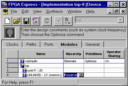
Figure 14- Unlinked LogiBLOX module set to "Preserve"
5.If one or more ports of the instantiated LogiBLOX are connected to a
top-level port, the "pad" direction must be specified. If the "pad" direction
is not specified, the following error messages can occur while implementing
the design:
Error: The pad mapping optimization can not determine the type of pad to
insert at the port '/top/DOtop<3>'. Please see the extended error message
for more details (FE-PADMAP-3)
Select the "Ports" tab within the Implementation window and define the "pad"
direction (input, output, inout, or 3-state) for any black-box instantiated
ports connected to top-level Verilog module ports. Ports of the black-box not
connected to a top-level port do not need their "pad" direction specified.
Under the "Pads" column, click and choose "Define..." from the pulldown menu.
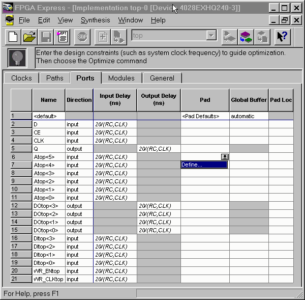
Figure 15- Defining Pads Step 1
Set the Pad Type to "Input" and give it a unique label like "Pad0".
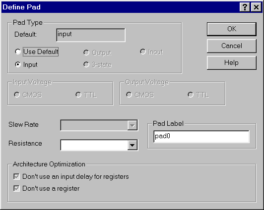
Figure 16- Defining Pads Step 2
You can use the label "Pad0" in the pulldown menu to define all the inputs.
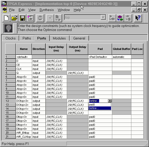
Figure 17- Defining Pads Step 3
Repeat the process for Output pads. Give this a unique name as well.
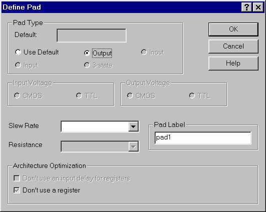
Figure 18- Defining Pads Step 4
Define all the ports connected to any LogiBLOX modules.
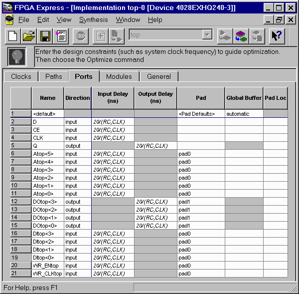
Figure 19- Defining Pads Step 8
6. Set all constraints for the rest of the design.
7. Optimize the design.
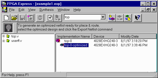
Figure 20- Design Optimized within FPGA Express
8.Write out the XNF file. Express will not write out a XNF file for the
instantiated LogiBLOX component.
9.Edit the pin directions of the instantiated LogiBLOX in the XNF file written
by Express. When Express writes out a XNF file that contains instantiated
black-boxes, Express writes the PIN directions for all the black-box pins as
"B". These pin directions must be corrected to the proper direction for the
given black-box. PIN directions can be I (input), O (output), or B
(bidirectional). If these are not corrected, M1 may not process the design prop
erly.
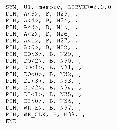
Figure 21- PIN records in XNF file, before modification
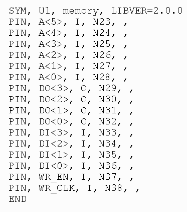
Figure 22- PIN records in XNF file, after modification
10.Take the XNF file written by Express and the .ngo file written by LogiBLOX
and process the design through the M1.3 Core Technology software.
Solution 3:
Instantiating an XNF file in VHDL or Verilog using FPGA Express v1.2 & M1.3
1. This procedure only works for Unified Library XNF files. Open the XNF file
with a text editor. Search for the string "LCANET". The LCANET line should
be either "LCANET, 5" or "LCANET, 6". If the search for LCANET turns up an
"LCANET, 4" or earlier, this XNF file cannot be used in the M1 flow.
Please see the M1 Conversion Guide for details on handling pre-Unified XNF
files (LCANET, 4 or earlier).
2. The name of the XNF file will be the name of the "component" instantiation
in the VHDL code, or the name of the "module" instantiation in the Verilog code.
3. To attach the XNF module in the VHDL/Verilog code, use the nets named in
the PIN records and/or SIG records in the XNF file as the port names of the
component instantiation. To reference buses in the instantiation of XNF
modules, the nets named in PIN records and/or SIG records must be of the form:
netname<number>. This will let the bus be referenced in the VHDL component as
a vector data type.
4. Using the filename of the XNF file as the name of the component, and the
name of nets in the XNF file as port names, instantiate the XNF file in the
VHDL/Verilog code.
5. Take all VHDL/Verilog design files, read, analyze, and implement the design
in FPGA Express. DO NOT read the XNF files into Express.
6. After implementing the design, select the implementation window and select
"modules". The instantiated XNF module will show up as "UNLINKED". Preserve
all instantiated "UNLINKED" modules.
7. VERILOG ONLY: If one or more of ports of the instantiated XNF are connected
to a top-level port, the "pad" direction must be specified. Select the
"Ports" tab in the Implementation window and define the "pad" direction
(input, output, inout, or 3-state) for any XNF instantiated ports connected
to top-level Verilog module ports. Ports of the XNF not connected to a
top-level port do not need to have a "pad" direction specified.
8. Set all constraints for the rest of the design.
9. Optimize the design.
10. Write out the top-level XNF file.
11. VERILOG ONLY: Edit the pin directions of the instantiated LogiBLOX in the
XNF file written by FPGA Express. When FPGA Express writes out a XNF file
that contains instantiated black-boxes, FPGA Express writes the PIN directions
for all the black-box pins as "B". These pin directions must be corrected to
the proper direction for the given black-box. PIN directions can be I (input),
O (output), or B(bidirectional).
12. Take XNF file from Express and XNF file instantiated in the VHDL/Verilog
code and process with M1.3.
Solution 4:
Miscellaneous Tips
(1) If the black-box module to be instantiated in a black-box design contains
I/O elements (IBUF, OBUF, OBUFT, IFD, etc.), care must be taken. Modules with
I/O for modular design will come in three types: modules with no I/O cells,
modules with I/O cells on all inputs and outputs, and modules with inputs and
outputs on some outputs. FPGA Express v1.2 has the capability to insert all
the I/O needed for a design, or none at all.
If the instantiated black-box contains one or more IO cells (like IBUF,OBUF,
OBUFT, IFD, ILD, OFD etc.), then all the IO cells in the top-level HDL design
must be instantiated. Additionally, FPGA Express must be prevented from
inserting I/O, by unselecting the "Do not insert I/O Pads" box in the "Create
Implementation" window in Express.
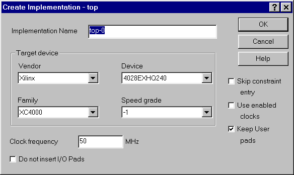
Figure 23- I/O not inserted
(2) FPGA Express will be unable to apply logical and timing constraints to
logic contained within black-boxes. This methodology places a "hole" in the
HDL/netlist, which will be filled when ngdbuild is run on the top-level file.
Since the contents of this hole are not visible to Express, FPGA Express will
be unable to apply M1 constraints to this module. For LogiBLOX RAM/ROM in
the modular design methodology, it is possible to apply logical and timing
constraints via a UCF. See (Xilinx Solution 2735) for more information.
(3) The M1.3 Core Technology software, like Verilog, is case-sensitive with
respect to names. VHDL is not case-sensitive, but the XNF written out by
FPGA Express will follow the case-sensitivity used in the VHDL code. If
case-sensitivity is not followed, M1.3 may not be able to properly merge the
FPGA Express XNF with the black-box modules instantiated in the VHDL code.
End of Record #2738
| For the latest news, design tips, and patch information on the Xilinx design environment, check out the Xilinx Expert Journals! |