Overview
LogiBLOX is a graphical interactive tool for creating modules, such as
counters, shift registers, and multiplexers. LogiBLOX includes both a library
of generic modules and a set of tools for customizing them.
The modules created by LogiBLOX can be used in designs generated with
schematic editors from Aldec, Viewlogic, Mentor Graphics, and Cadence,
as well as third-party synthesis tools such as Synopsys FPGA Compiler,
Xilinx Foundation Package,
and Mentor Autologic.
LogiBLOX modules are used whenever you need a customized version of
a standard function. For example, with a LogiBLOX counter, you start with
a generic template for a counter and tailor its functionality to your needs.
In contrast, a standard ready-made counter has a previously defined set
of functions and in the case where you want a counter with specific capabilities,
you would need to have available a library of different counters, one of
which contains the functions you need.
Simulation of LogiBLOX modules can be performed using behavioral VHDL,
Structural Verilog or Gate level EDIF models.
The LogiBLOX graphical user interface (GUI) is available directly from
supported schematic editor packages. LogiBLOX also supports synthesis-based
tools by either letting the synthesis tool infer modules from the HDL code,
or by letting you specify the module with the LogiBLOX Module Selector
in its stand-alone mode and then instantiating it in your HDL design.
LogiBLOX modules are created to take full advantage of the architecture
being targeted. Supported architectures are the XC3000A, XC3100A, XC4000E,
XC4000EX and XC5200 device families.
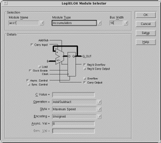
LogiBLOX Module Selector
Advantages of using LogiBLOX
LogiBLOX includes the following features that enhance design entry and
module processing:
LogiBLOX Design Entry Features
-
LogiBLOX eases design entry by allowing you to tailor complex logic blocks
to precisely match your design¹s needs.
-
The LogiBLOX graphical user interface allows you to quickly and easily
specify complex modules with the assistance of interactive Design Rule
Checker (DRC) checks and prompts.
-
An image of the module with the specified pins and attributes is updated
each time you activate a module attribute or connection in the Module Selector.
-
The graphical user interface automatically disables selections that are
incompatible with your current design selections.
LogiBLOX Processing Features
-
In a synthesis-based environment, the modules you create with LogiBLOX
are implemented as you incorporate them into the rest of your design.
-
In LogiBLOX, a simulation model (VHDL, EDIF, or Verilog) is generated for
each LogiBLOX module during design entry. This enables immediate simulation
of LogiBLOX design without logic implementation. The behavioral functional
model is produced as you enter the LogiBLOX module in your schematic.
-
Many synthesis tools automatically infer LogiBLOX modules. You can also
incorporate LogiBLOX modules in HDL designs through instantiation without
compromising behavioral simulation support.
-
Modules are synthesized quickly "on-the-fly" by the LogiBLOX module compiler.
LogiBLOX Modules
 to view the to view the  PDF files below. PDF files below.
Download datasheet version of this page.
LogiBLOX modules are listed below by function:
| Modules |
Function |
| ACCUMULATOR |
Adds data to or subtracts it from the current value stored in the acculator
register. |
| ADDER/SUBTRACTER |
Adds or subtracts two data inputs and a Carry input. |
| COMPARATOR |
Compares the magnitude or equality of two values. |
| COUNTER |
Generates a sequence of count values. |
| Logic |
| CONSTANT |
Forces a constant value onto a bus.Forces a constant value onto a bus. |
| DECODER |
Routes input data to 1-of-n lines on the output port. |
| MULTIPLEXER |
Routes input data on 1-of-n lines to the output port. |
| SIMPLE GATES |
Implements AND, INVERT, NAND, NOR, OR, XNOR, and XOR logic functions. |
| TRISTATE |
Creates a tri-stated data bus. |
| I/O |
| INPUT/OUTPUT |
Connects internal and external pin signals. |
| PAD |
Simulates an input/output pad. |
| Sequential |
| CLOCK DIVIDER |
Generates a period that is a multiple of the clock -input period. |
| COUNTER |
Generates a sequence of count values. |
| SHIFT REGISTER |
Captures the input data on active Clock transitions. |
| Storage |
| DATA REGISTER |
Captures the input data on active Clock transitions. |
| MEMORY: ROM, RAM, SYNC_RAM, DP_RAM |
Stores information and makes it readable. |
| SHIFT REGISTER |
Shifts the input data to the left or right. |
|