| Foundation
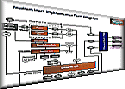
Series Implementation Flow Overview:
1. Start the Foundation Project Manager
Click the Xilinx Foundation Series Project Manager icon on
your Windows desktop. Alternatively, you can use the
Start Menu link, found under Start Menu >
Programs > Xilinx Foundation Series > Project Manager.
2. Create a design project
Using File > New, create a project, which will contain all of the design
and device implementation files.
3. Enter your design
You can use one or more of Foundations
design entry tools to capture your design:
Schematic Editor, HDL Editor, and State Editor.
Each of these tools is accessible
from the Project Managers Flow Diagram,
found on the first tab of the Project Managers
right-hand pane. Top-down and
bottom-up design techniques are supported.
4. Simulate your designs functionality
Click on the Functional Simulation button in the Flow Diagram. This
will start the gate level simulator. You
can select signals to be monitored in your simulation
by either adding probes to nets and buses in the schematic
view ( using Mode > Test Points ), or by
adding signals in the simulator (using Signal > Add Signals
)
5. Implement your design in a Xilinx device
Select the Implement button in
the Flow Diagram. The Design Manager window allows you to run the
Xilinx Implementation Tools, and also
manage netlist versions and
the corresponding implementation revisions
of your design . By selecting Design > Implement, you
can start the process of implementing your design.
6. Verify your designs timing
Using the gate level simulators Timing mode, you can now simulate
the timing-annotated design files created by the Implementation Tools.
To start the gate level simulator in Timing mode,
select Timing Simulation in the Flow Diagram.
You also have the option of using the Interactive Timing Analyzer to
perform static timing analysis of your design. The ITA can
be accessed from the Design Manager by selecting Tools
> Timing Analyzer.
7. Download your design into the part
Using either the Hardware Debugger (FPGA) or JTAG
Download (CPLD) software, download the implemented design into your Xilinx
device. These tools are accessed from the Design Managers Tools
menu.
Xilinx
Recommended Settings:
Device
Architecture Support:
| FPGA |
XC4000E/L |
|
XC4000X (EX/XL/XV) |
|
Spartan |
|
XC5200 |
|
XC3X00A |
| CPLD |
XC9500 |
|