| Foundation
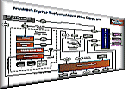
Express Implementation Flow Overview:
1. Create a Project
Click the New Project button to create a project.
All HDL files processed by Foundation Express must be done
through a project.
2. Add HDL files to a project and analyze HDL files
After creating a project, HDL files for the design can be added
to the project by clicking the Add Source button. After
adding the HDL files for the design, Foundation
Express will automatically analyze the HDL files.
3. Implement the design
Select the top-level module/entity in the Design Sources window,
then click the implement button and specify the
target package, part, and speed grade.
4. Enter Constraints
In the Chips window, select the implementation. Right-click
on the selected implementation and select
Edit Constraints. The constraints window will appear
for that implementation. Edit the necessary constraints, and close
the constraints window.
5. Optimize the Design
With the desired implementation selected in the Chips
window, click the optimization button.
6. Write Out Detailed Design Report
Information on the design hierarchy,
inferred operators, cell count, timing constraints and clock
speed estimates is available by clicking on the Project Report button.
7. Write Out an XNF File and Place and Route With F1.4
After optimization is complete, click on the Export Netlist button.
Open the Foundation Series Design Manager (Start -> Programs -> Xilinx
Foundation Series -> Design Manager) and identify the XNF netlist as the
Input Design source.
Foundation
Express Tips:
1. Control Finite State Machine (FSM) Encoding
The default FSM encoding style is
set in the Synthesis -> Options -> Project window.
One-Hot encoding is recommended for FPGAs, Binary encoding is recommended
for CPLDs.
2. Perform Static Timing Analysis and Debugging
Static Timing Analysis may be performed on optimized designs.
Select the design in the Chips window, right-click
and select View results. You can view estimated
performance and other critical path information, I/O setup
and clock-to-output timing as well as detailed area reports
3. Achieve optimum Synthesis performance
Optimum synthesis results can be driven
using the Create Implementation dialog
box. Selecting the speed option will
synthesize a design to optimize for highest speed. Selecting the area option
will give minimal area.
Device
Architecture Support:
| FPGA |
XC4000E/L |
|
XC4000X (EX/XL/XV) |
|
Spartan |
|
XC5200 |
|
XC3X00A |
| CPLD |
XC9500 |
|