 |
Tech
Topics
|
|
|
Virtex Delay-Locked
Loops (DLL)
Supporting the highest bandwidth data rates between devices
requires advanced clock management technology such as digital
delay-lock loops (DLLs). The DLL circuitry allows for very precise
synchronization of external and internal clocks. Xilinx was
the first to deliver DLLs in programmable logic by offering
four 200 MHz DLLs in every Virtex device. Figure 1 (Click here
to view the figure) shows the block diagram of the DLL circuitry.
The Virtex-E family takes this technology to the next level
with devices containing eight DLLs capable of over 311 MHz.
Virtex Series DLLs provide precise clock edges through phase
shifting, frequency multiplication, and frequency division.
The precise duty cycle generation is critical for high performance
applications (like Double Data Rate, or DDR) in which a slight
shift in duty cycle can dramatically decrease overall system
performance.
|
Material pertains to all Virtex series devices unless specifically noted.
For more technical details including the graphics and waveforms, click
here to download the PDF version.
History
Phase-locked loops (PLL) have been used since the 1940's in analog implementations.
Recent emphasis on digital methods has made it desirable to match signal phases
digitally. A digital delay-locked loop (DLL) in place of an analog PLL eliminates
the need for separate noise-free ground and power planes. Virtex DLLs also ensures
a reliable frequency range over all variations of manufacturing processes, temperature
and voltages.
DLL Benefits
The Virtex FPGA series provides up to eight fully
digital dedicated on-chip DLL circuits which provide system clock generation,
deskewing of clock signals distributed throughout the device and/or the board,
and other advanced clock domain control. In addition to frequency synthesis, a
DLL optionally provides duty cycle correction and phase shift. Digital Delay
Locked Loops provide significant system benefits:
- Achieving zero clock skew, effectively eliminating the clock-distribution
delay and allowing digital closed-loop control. This control provides
system clock rates ranging from 25 to 320 Megabits per second (Mbps)
with 100 ps resolution. A DLL greatly reduces the clock latency of a
device, which in turn reduces the clock-to-out timing.
- Precise control of system clocks, both internally at the device level
as well as externally for other devices on the board using the independent DLLs
per Virtex or Virtex-E device.
- Clock mirroring on the PCB to synchronize external chips. This also
reduces system cost by eliminating the need for external devices (like
the Roboclock device from Cypress ). DLLs support clock mirroring with
less than 100 Ps skew.
- Multiply or divide the external clock to produce a clock to use on
or off the chip, allowing for multiple clock domains. Designers can
also use the DLL to phase-shift clocks in order to support clock multiplexed
systems.
- 2X-4X: Double or quadruple the incoming clock frequency, supporting designs
that need a fast internal operation but a slower external clock. This gives the
designer a number of choices. For example, clocks routed on the board can be kept
to lower frequencies thus avoiding signal-to-noise issues while the FPGA runs
at maximum speed at the same time. All multiplied clocks have synchronized edges.
On chip clock speeds can be high as 320 MHz
- CLK_DV: Divide clock by 1.5,
2, 2.5, 3, 4, 5, 8 or 16. The optional 50/50 duty cycle correction is available
as well. Often times applications monitor data at a high frequency, but process
data at a much lower clock frequency (e.g. read data at 155 MHz, process data
at 38.5 MHz).
- Support clock multiplexed applications by
creating 4 quadrant clock phases (0/90/180/270). Input four sequential bits per
clock period. DLL Phase shift. Used with the clock divider (e.g. data is applied
at 200 MHz and registered at 50 MHz by four clocks shifted 90 degrees each).
- Selectable
division values
- 1.5, 2.0, 2.5, 3, 4, 5, 8, or 16
- 50/50 duty cycle
correction available
- Use DLL pair to combine functions
- Delivers
superior chip-to-chip clock performance
- Up to 622 Mbps LVDS and LVPECL
performance on 36 Virtex-E I/O pairs
- SelectLink technology for high
speed DDR Virtex-to-Virtex device communication
- 200 Mbps Virtex-to-Virtex
device
- 311 Mbps for Virtex-E device to Virtex-E device
(up to 804 pins)
- 143 MHz ZBT SRAM, 200 MHz for Virtex-E device
- 125
MHz SDRAM/SGRAM, 133 MHz SDRAM.
- Use precise 50/50 duty cycle to achieve
high-speed DDR interface to external devices
- 200 MHz Virtex Double Data
Rate
- 266 MHz Virtex-E Double Data Rate
- Supplies
flexible power management. Analog PLLs require a continuous clock. On the other
hand, designers can use DLL techniques to stop, and then restart, the clock without
acquiring a new lock, which would require several microseconds. This feature allows
a designer to build a "power save" mode into the final application.
- Provides greater stability. DLLs operate reliably on waveforms with
up to 1 ns frequency drifts adding a maximum of only 60 Ps jitter. This
stability is far beyond the typical 100 PPM (0.01%) of most oscillators,
where any input jitter is reflected on the output.
Most discrete PLLs are designed with a specific application
in mind. Once external pins are connected to resistors, capacitors, power, and
ground, the designer must insure no signal couples into or interferes with these
pins. Any noise may result in either high jitter or the PLL not locking. Otherwise,
the designer can experience significant signal integrity problems. On today's
high-speed circuit boards this puts an additional burden on the design and layout
engineer to provide separate power and ground connections.
Eight High Performance DLLs
Drop-in Bandwidth Optimization with Virtex-E devices
Supporting high bandwidth
data rates between devices requires advanced clock management technology offered
by DLLs. Table 1 summarizes the bandwidth critical parameters of the Virtex-E
DLL. The DLL circuitry allows for very precise synchronization of external and
internal clocks. DLLs also provide precise clock edges during phase shifting,
frequency multiplication, and frequency division. Precise duty cycle generation
is critical for high performance applications, such as Double Data Rate (DDR)
where a slight shift in duty cycle can dramatically decrease overall system performance.
The Virtex-E family offers 8 DLLs, allowing both internal and external de-skew
of 4 systems clocks.
| Parameter | Value | | Maximum
Output Frequency | 320 MHz* | | Maximum
Output Jitter |
100 Ps |
| Output
Frequency Duty Cycle |
50% +/- 100 Ps |
| *
Based on Virtex-E -7 speed grade product |
| Table
1: Bandwidth Critical specifications of the Virtex-E DLL |
Maximize DDR Bandwidth
A key technique for increasing the bandwidth of a particular data port
is to have signals change on both edges of a clock, commonly referred
to as the Double Data Rate technique. Memory suppliers have already started
to support this type of high performance technique to increase the memory
bandwidth of their devices. At high frequencies, signal integrity limits
the clock performance, which limits the bandwidth of the data. Bandwidth
for the port is immediately doubled if the architecture can change data
at each edge of a system clock. A precise 50 percent clock duty cycle
is critical for this technique. Since Virtex-E DLLs can generate clocks
with a duty cycle guaranteed to be within 100 Ps of 50 percent, system
designers can achieve the maximum memory bandwidth in the DDR application.
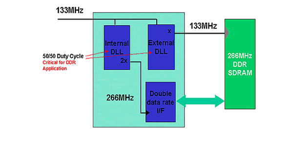
The following diagram demonstrates how Virtex-E DLLs help achieve maximum
bandwidth in a 266 MHz DDR application. The diagram below demonstrates
how Virtex-E DLLs help achieve maximum bandwidth in a 266 MHz DDR application.
Virtex Advantages
A comparison of the performance
and flexibility of DLLs versus PLLs in table 2 shows the value designers obtain
as they use the Xilinx Virtex Series. DLLs are beneficial for designers who
require external interface performance above 50 MHz. This includes interfacing
to memory devices in numerous applications, as well as networking and telecommunications
applications. DLLs are superior for designs that have a clock fan-out of greater
than 10, or when multiple clocks are required. DLLs are critical to achieve maximum
performance for Double Data Rate (DDR) applications. Two DLLs are required for
complete internal and external clock deskew. With 8 DLLs, Virtex-E allows 4 system
clocks to be managed. Alteras APEX E family has only 2 or 4 PLLs, and only 1
PLL in their APEX family. Only 2 of the maximum 4 PLLs available on the Altera
APEX E product support LVDS. All 8 DLLs on Virtex-E support LVDS. DLLs do not
require separate power and ground planes. Alteras APEX and APEX E families PLLs
require designers to use PCBs with separate noise-free power and ground planes. - DLLs
are beneficial for designers who require external interface performance above
50 MHz. This includes interfacing to memory devices in numerous applications,
as well as networking and telecommunications applications.
- DLLs are superior
for designs that have a clock fan-out of greater than 10, or when multiple clocks
are required.
- DLLs are critical to achieve maximum performance for Double
Data Rate (DDR) applications. o Two DLLs are required for complete internal and
external clocks de-skew. With 8 DLLs, Virtex-E allows four system clocks to be
managed. Altera's APEX E family has only two or four PLLs, and only one PLL in
their APEX family.
- All eight DLLs on Virtex-E support LVDS. Only two
of the maximum four PLLs available on the Altera APEX E product support LVDS.
- DLLs do not require separate power and ground planes. Altera's APEX and
APEX E families' PLLs require designers to use PCBs with separate noise-free power
and ground planes.
| Feature | Virtex | Virtex-E | APEX | APEX
E | | Architecture | DLL | DLL | PLL | PLL | | Technology | 100%
Digital | 100% Digital | 100%
Analog | 100% Analog | | Quantity | 4 | 8 | 1 | 2
- 4 | | Max. Output (MHz) | 200 | 311 | 133 | 200 | | Input
Duty Cycle | N/A | N/A | 40
- 60% | 40 - 60% | | Output Duty
Cycle |
50% +/- 100 Ps |
50% +/- 100 Ps |
40 - 60% | 40 - 60% | | Min.
Input Clock (MHz) | 25 | 25 | 5 | 5 |
| Table
2. Virtex DLL versus APEX PLL Technology |
Customer Comments
"Virtex FPGAs have allowed us to implement
our next generation digital TV broadcast systems in record time," said John Simmons,
project manager, of NDS, a world leader in digital broadcasting solutions. "A
key time saver was the availability of multiple DLLs that allowed us to synchronize
a 74 MHz clock to more than 30 devices including multiple FPGAs, SDRAMs, and other
components. Designing a no-skew clock system from scratch would take months. Xilinx
delivered a ready-made solution to us with Virtex FPGAs."
"Virtex FPGAs have aided us in deserializing the Rambus control and
data buses into a parallel format," said Brauer. Virtex devices accept
Rambus data after presampling logic has converted the serial channel from
26 bits on both edges at 800 Mbps to 56 single edge signals to 400 Mbps.
"Tektronix has been successful at using the Virtex FPGA to accept this
400 Mbps data directly into the Virtex device." This was achieved by providing
multiphase clocks to the device (four phases). Each clock was connected
to a different global clock input, routed over its own internal global
route with separate DLL's (digital delay lock loops).
References
Related Xilinx Documents
 to view the
  PDF files below.
|