System Overview
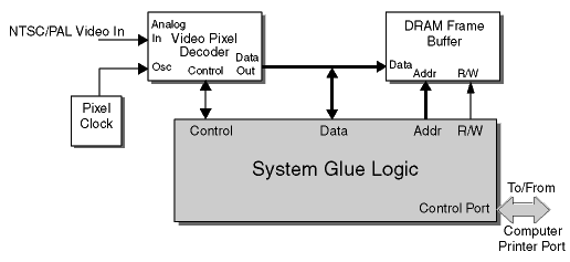
The basic functional organization of a high-volume video capture system
is shown in Figure 1. This architecture is commonly found in low-end frame-grabber
products that range in price from $60 to $100. Examples of such products
include Grab It from AIMS Labs, Snappy from Play Inc. and the Dazzle
Digital Video Creator from Dazzle Multimedia. There are three major functional
blocks: The video pixel decoder (VPX), a frame buffer and system glue logic.
The VPX digitizes the analog video source, whether it be from a camcorder,
VCR or CCD camera. The result is a sequence of pixels that, once assembled
into a frame, constitute one complete video picture. The frame is stored
in the buffer until it can be sent to the PC. The system glue logic consists
of all the logic necessary to coordinate the flow of pixels from the VPX
to the buffer and, again, from the buffer to the printer ( parallel) port.
Figure 1 Video Capture System Block Diagram
The components used to realize the three main functional blocks of the
demo board were chosen for their low cost as well as their performance
characteristics. They are all 5V CMOS devices employing the TTL signal
standard. The VPX 3214 C from ITT performs the video pixel decoder
function. A 1,048,576 x 16-bit asynchronous DRAM from LG Semicom
serves as the frame buffer. A Spartan FPGA, otherwise referred to
as the Spartan control unit, contains all the system glue logic. The three
devices share a common 16-bit bidirectional bus managed by the Control
Unit, which also presides over an independent 8-bit bus leading to the
parallel port. The two analog video inputs connect directly to the VPX.
Basic Operation
The VPX samples the incoming analog video signal at a rate of 20.25 MHz,
digitizes it and converts it to a stream of pixels in the YCbCr format
(4:2:2). The Spartan control unit transfers the pixels from the VPX down
the 16-bit bus to the frame buffer. The process by which this transfer
takes place combines odd and even fields to produce non-interlaced frames
suitable for display on the PC monitor. Using a "write counter" to generate
addresses, a frame is written to the buffer then overwritten with a new
frame in cyclical fashion.
The PC requests the acquisition of a frame through the parallel port.
The control unit responds by accessing pixels from the buffer according
to addresses generated by a "read counter". Then it matches the 16-bit
pixels to an 8-bit bus and sends them through the parallel port to the
PCs memory.
Board Capabilities
The board has two analog video inputs permitting two composite sources
(i.e., NTSC and PAL) or one component source (i.e., S-VHS). The NTSC,
PAL, SECAM and S-VHS standards are all supported. These standards are automatically
identified at the inputs to the VPX. One source at a time is selected for
sampling.
The output from the board is an 8-bit-wide, non-interlaced, digital
video stream in the YCbCr (4:2:2) format. This output is transferred to
the PCs memory via the parallel port (EPP protocol) at 2 Mbytes/sec. The
parallel port permits connection not only to desktop PCs but also notebook
computers. Of the interfaces common to both machines, this port provides
the highest bandwidth. Nevertheless, to support real-time video transmission,
still faster interfaces, such as the PCI for desktop machines or the PCMCIA
for portables should be considered.
The Video Pixel
Decoder
The VPX 3214 C performs a number of functions pertaining to video acquisition,
including automatic standard detection, sampling of the analog source,
conversion to digital YcbCr 4:2:2 format, generation of synchronization
signals and frame resizing. The internal organization of this 44-pin device
is shown in Figure 2.
Figure 2. The VPX 3214 C Video Pixel Decoder
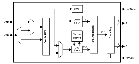 Note: Only those features used on the demo board are shown.
A set of control registers connected to an I2C bus determines
the various modes of operation. This bus consists of two lines: a clock
line (SCL) and a bidirectional serial data line (SDA). Since the I2C
driver connected to SDA is open-drain, a pull-up resistor is required.
The control unit, in the role of master, configures the VPX 3214 C after
power-up.
The four analog video inputs, labeled VIN, VIN2, VIN3, AND CIN, support
a variety of standards in different combinations. The demo board
uses two of the inputs: VIN1 accepts composite (CVBS), luma (Y), and chroma
signals. VIN2 takes CVBS and Y. In a composite video application,
the board can switch between any combination of NTCS, PAL or SECAM sources
at VIN1, and VIN2. In a component video application (i.e., S-VHS),
the chroma signal goes to VIN1 and the luma signal goes to VIN2.
These selections are made in internal registers that are controlled using
the I2C bus.
A 20.25 MHz crystal synchronizes all operations within the VPX 3214
C including sampling of the selected analog video source. Two 8-bit
ADCs convert the samples to digital YCbCr 4:2:2 format. For a composite
video source, this process entails color decoding to separate the chroma
and luma signals. One 16-bit pixel is sampled every cycle whereas
Cb and Cr are sampled every other sample. Each pixel in the sampled
sequence is composed of an 8-bit luma component and an 8 bit chroma component.
The latter alternates between Cr and Cb in going from one pixel to the
next. Following analog to digital conversion, there are 1056 pixels
in each line of video. A horizontal resizing feature that lowers
the effective sampling rate can be used to decrease the number as low as
32 pixels line.
The number of lines in a video frame (i.e., the complete picture), varies
according to the standard in use: 525 for NISC and 625 for PAL/SECAM.
Analog video sources are typically interlaced which means that the frame
is decomposed into two fields, each with half the number of lines.
The video signal is transmitted as a sequence of even and odd fields.
The original picture is recreated by alternating lines from one such pair
of fields. Vertical resizing (i.e., compression) is possible by dropping
lines. On the VPX 3214 C, both vertical and horizontal resizing
are controlled using the I2C bus.
The ability to reduce the size of the video picture by changing the
number of pixels both horizontally and vertically helps reduce the frame
buffers capacity requirements as well as the computer interfaces bandwidth
requirement.
The VPX 3214 C has two 8-bit output ports, labeled A and B. The
demo board uses both to transfer pixels on to a 16-bit bus. The output
enable line /OE provides three-state control for A and B. In what is known
as the synchronous transfer mode, the VPX drives the 20.25 MHz sampling
clock (PIXCLK) on to the board for the purpose of synchronizing pixels.
A number of flag signals are available for coordinating the timing of
external components on the demo board. (The polarity of the signals
listed below is programmable. For the sake of clarity, only one polarity
is described for each signal.) VACT is High in the presence of valid data
on ports A and B. HREF, the horizontal reference signal, is inferred
from the video source. It is High for the fixed period during which
the 1,056-pixel horizontal line is being transferred through the ports.
If the number of valid pixels equals 1,056, then the pulses on VACT and
HREF are identical. In cases where the number of valid pixels is
less than 1,056 (i.e., horizontal resizing), the VACT pulse will be shorter
than the HREF pulse. VACT will be Low for dropped lines (i.e., vertical
resizing). VREF, the vertical reference signal, is inferred from the video
source. It provides a High pulse at the beginning of each field (both odd
and even). ODD/EVEN, sampled on the falling edge of VREF, is Low for even
fields and High for odd fields. The signals VACT, HREF, VREF and ODD/EVEN
are provided as inputs to the control unit.
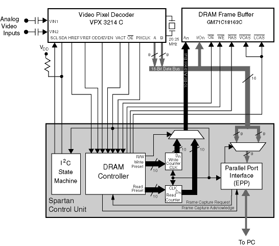
The Spartan Control Unit
A Spartan FPGA is used to implement the following functions: a DRAM controller
(with DMA), a parallel port interface (the EPP protocol) and an I2C
state machine. How these functions are organized internally, as well
as how they connect to the VPX and the DRAM chips is shown in figure 3.
Each of the functions is now described in more detail.
Figure 3. Detail of the Spartan Control Unit
DMA Operation
Associated with the DRAM controller are two 10-bit counters, one generates
addresses for writing pixels to the DRAM, the other generates addresses
for reading pixels from the DRAM. These counters make up a DMA circuit
that permits sequential addressing of the DRAM at a rate of 20.25 MHz.
The DRAM controller uses the Write Preset and Read Preset buses shown in
Figure 3 to load start and stop addresses into the counters. These serve
to delimit the range of DRAM addresses that can be accessed. The
difference between the start and stop addresses is set equal to the number
of pixels in a frame. For the VPX 3214 C, the maximum number is 1056
pixels/line by 625 lines/frame (PAL standard) or 660 K-pixels. The
addresses of the two counters are multiplexed to a 10-bit address bus leading
to the An inputs on the DRAM chip. The DRAM controller uses a R/W
line to select between a write address for loading pixels from the VPX
and a read address for transferring to the parallel port interface.
DRAM Controller
The DRAM controller performs two basic functions: First, it coordinates
the transfer of pixels from the VPX to the DRAM. Second, it coordinates
the transfer of pixels from the DRAM to the parallel port interface (within
the Spartan device).
VPX-to-DRAM Transfers
The technique of direct memory access (DMA) is used to transfer pixels
from the VPX to the frame buffer. The DRAM controller uses the video synchronization
signals from the VPX, specifically HREF, VREF, ODD/EVEN and VACT, to generate
the strobe lines necessary for writing the pixels into the DRAM, namely
/RAS, /UCAS, /LCAS, /WE, and /OE. The VPX continuously places pixels on
the bus at a rate of 20.25 MHz. As soon as the VPX puts a pixel onto the
16-bit data bus, the DRAM writes it into memory.
The video data is commonly organized as a succession of alternating
odd and even fields. At the time of display, video systems will interlace
each pair of fields together to form a frame (i.e., a complete picture).
Computer systems, on the other hand, display video in non-interlaced form.
Therefore, the odd and even fields coming from the VPX need to be digitally
interlaced together to form frames. The DRAM controller accomplishes
this by switching an address bit outside of the write counter that discriminates
between odd and even lines in the frame buffer. If possible, the
frame is stored in more-or-less the same form in which it will be displayed
with each horizontal video lines occupying sequential rows of memory, always
starting and ending at the same columns. In this way, managing the
address space is greatly simplified. For example, a 1024 x 625 pixel
image (with horizontal resizing) will just fit the maximum row length (no
wrapping), occupying a grid of 1024 columns by 625 rows. According to the
level on ODD/EVEN, the DRAM controller will switch an address line so pixels
belonging to odd fields will go to odd rows in the frame grid and pixels
belonging to even fields will go to even rows. In this way, video frames
are continuously constructed from odd and even fields. As soon as a frame
is complete, the DRAM controller proceeds to overwrite it as part of an
ongoing, cyclical process. Writing pixels to the DRAM at a rate of 20.25
MHz is sufficient to refresh the DRAM.
DRAM-to-Parallel-Port Transfers
The second function of the DRAM controller is to transfer pixels from the
frame buffer to the parallel port interface. As was the case for the first
function, DMA is used here as well. The PC requests a video frame through
the parallel port interface, which activates the Read Buffer Request
line. In response, the DRAM controller monitors VREF and ODD/EVEN
for an indication that the entire frame has been written to the DRAM.
Then, it desserts the DRAMs write enable (/WE) and loads the start address
into the read counter, which it now selects to drive An. Ports A
and B on the VPX are put into a high impedance state as the I/On lines
on the DRAM, now configured as outputs, are enabled. The DRAM controller
activates the Read Buffer Acknowledge line to inform the parallel port
that the frame is ready for transfer to the PC, then it toggles the /RAS,
/UCAS and /LCAS lines to access pixels at a rate of 1M pixel/sec. (This
is sufficient for refreshing the memory). In contrast to the write
counter, which generates addresses for the VPX-to-DRAM function that skip
every other row in memory, the read counter generates addresses for the
DRAM-to-Parallel port function row-by-row. The pixels are transferred
from the DRAM to the 16-bit data bus. Upon entering the Spartan device,
they are matched to an 8-bit bus. From here, the parallel port interface
sends them to the PC using the EPP protocol (2MBytes/sec).
Spartan Configuration
After power-up, the configuration file for the control unit is downloaded
from the PC through the parallel port to the demo boards Spartan device.
For the purposes of configuration, the parallel port uses the compatibility
mode, a subset of the EPP protocol, to download the configuration data.
This mode is effectively the same as the Centronics parallel interface,
which transfers data in one direction from the host computer to the demo
board. (During operation, the board makes use of the enhanced port features
such as bidirectional data transfer). Eight lines, D0 - D7, are available
for carrying data, though, since the 5V Spartan device is configured in
serial fashion, only D0 is used. The host asserts a signal called
/STROBE to indicate the presence of valid data. The peripheral responds
by activating a BUSY signal, then acknowledges receipt of a byte by going
LOW on /ACK. It finally indicates that it is ready to receive the next
byte by releasing both BUSY and /ACK. The interface has other lines
ordinarily use to control a printer. Of these, /INITIALIZE-PRINTER, SELECT,
and OUT-OF-PAPER are used for hand shaking between the parallel port and
the Spartan device.
The slave-serial configuration mode is selected by tying the MODE pin
on the Spartan device High. Using this mode, configuration of the
FPGA is under the control of the host computer. A Low pulse on the
/PROGRAM pin clears the device. As soon as the FPGA is ready to receive
configuration data, it drives the /INIT pin High. Then, the configuration
data is serially written to the DIN pin, synchronized to a clock signal
applied to the CCLK pin. When the device is full, its DONE pin goes High,
signifying that configuration is finished.
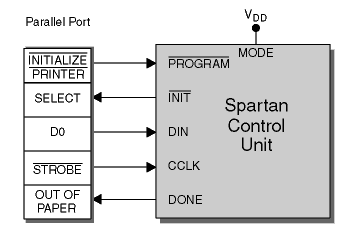
The connections between the parallel port and the Spartan configuration
pins are shown in Figure 4. The parallel port signal /INITIALIZE-PRINTER
strobes the Spartan devices /PROGRAM pin to initiate configuration. After
the Spartan devices /INIT line pulls SELECT High, D0 on the parallel port
carries the configuration data to DIN on the Spartan device. /STROBE
provides a clock signal for CCLK. Since the PC sends a continuous
stretch of bits through the parallel port with uniform timing, the BUSY
and /ACK signals are unnecessary. At the end of configuration, the DONE
pin drives the OUT OF PAPER line High.
Figure 4. Connections between the Parallel Port and
the Spartan Device
|