|
Family Extended to 200,000 Gates
You asked for it and we listened! We are proud to announce the latest addition to our popular Spartan-II family: the XC2S200. As high-volume designs grow more complex, the need for higher density, increased memory, and greater I/O count grows as well. For these designs, the XC2S200 fits the bill by featuring up to 200,000 system gates, 14 total RAM blocks, and up to 284 I/Os in three low-cost, high-volume packages: PQ208, FG256, and FG456. With the XC2S200, you'll get 36% more logic cells compared with the XC2S150 and five times the density of the largest Spartan or Spartan-XL device.
The XC2S200 includes all the features that make the Spartan-II solution a winning one:
- Distributed and Block Memory
- Four Digital Delay Locked Loops per Device
- Versatile I/O Interface Technology
- Full PCI Compliance
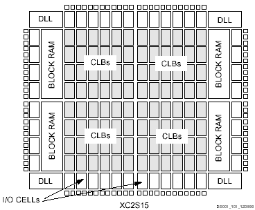
Spartan-II Architectural Features
Block Diagram
The Spartan-II family of Field Programmable Gate Arrays (FPGAs) is implemented with a regular, flexible, programmable architecture of Configurable Logic Blocks (CLBs), surrounded by a perimeter of programmable Input/Output Blocks (IOBs), interconnected by a powerful hierarchy of versatile routing resources. The architecture also provides advanced functions such as Block RAM and clock control blocks.
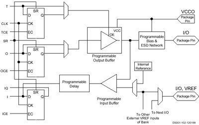
Input/Output Block
The Spartan-II IOB features inputs and outputs that support 16 I/O signaling standards, including LVCMOS, HSTL, SSTL, and GTL. These high-speed inputs and outputs are capable of supporting various state-of-the-art memory and bus interfaces. The three IOB registers function either as edge-triggered D-type flip-flops or as level sensitive latches. Each IOB has a clock signal (CLK) shared by the three registers and independent clock enable (CE) signals for each register. In addition to the CLK and CE control signals, the three registers share a Set/Reset (SR). For each register, this signal can be independently configured as a synchronous Set, a synchronous Reset, an asynchronous Preset, or an asynchronous Clear.
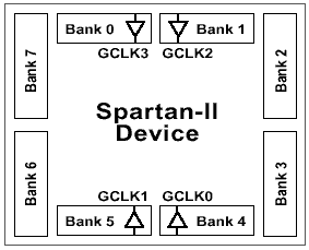
Banking of I/O Standards
Some of the I/O standards require VCCO and/or VREF voltages. These voltages externally are connected to device pins that serve groups of IOBs, called banks. Consequently, restrictions exist about which I/O standards can be combined within a given bank. Eight I/O banks result from separating each edge of the FPGA into two banks. Each bank has multiple VCCO pins, all of which must be connected to the same voltage. This voltage is determined by the output standards in use.
In TQ144 and PQ208 packages, all VCCO pins are bonded together internally, and consequently the same VCCO voltage must be connected to all of them. In the CS144 package, bank pairs that share a side are interconnected internally, permitting four choices for VCCO. In both cases, the VREF pins remain internally connected as eight independent banks.
Logic Cells
The basic building block of the Spartan-II CLB is the logic cell (LC). An LC includes a four-input function generator, carry logic, and a storage element. The output from the function generator in each LC drives both the CLB output and the D input of the flip-flop. Each Spartan-II CLB contains four LCs, organized in two similar slices. In addition to the four basic LCs, the Spartan-II CLB contains logic that combines function generators to provide functions of five or six inputs. Consequently, when estimating the number of system gates provided by a given device, each CLB counts as 4.5 LCs.
Spartan-II function generators are implemented as 4-input look-up tables (LUTs). In addition to operating as a function generator, each LUT can provide a 16 x 1-bit synchronous RAM. Furthermore, the two LUTs within a slice can be combined to create a 16 x 2-bit or 32 x 1-bit synchronous RAM, or a 16x1-bit dual-port synchronous RAM. The Spartan-II LUT can also provide a 16-bit shift register that is ideal for capturing high-speed or burst-mode data. This mode can also be used to store data in applications such as digital signal processing. The storage elements in the Spartan-II slice can be configured either as edge-triggered D-type flip-flops or as level-sensitive latches.
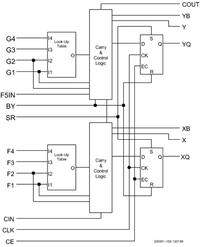
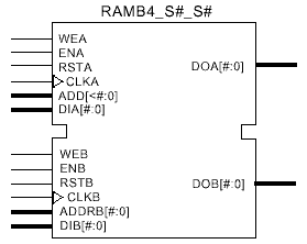
Block RAM
Spartan-II FPGAs incorporate several large Block SelectRAM+ memories. These complement the distributed SelectRAM+ resources that provide shallow RAM structures implemented in CLBs. Block SelectRAM+ memory blocks are organized in columns. All Spartan-II devices contain two such columns, one along each vertical edge. These columns extend the full height of the chip. Each memory block is four CLBs high, and consequently, a Spartan-II device 8 CLBs high will contain 2 memory blocks per column, and a total of 4 blocks.
Delay-Locked Loop
Associated with each global clock input buffer is a fully digital Delay-Locked Loop (DLL) that can eliminate skew between the clock input pad and internal clock input pins throughout the device. Each DLL can drive two global clock networks. The DLL monitors the input clock and the distributed clock, and automatically adjusts a clock delay element. Additional delay is introduced such that clock edges reach internal flip-flops exactly one clock period after they arrive at the input. This closed-loop system effectively eliminates clock-distribution delay by ensuring that clock edges arrive at internal flip-flops in synchronism with clock edges arriving at the input.
Configuration
Configuration is the process by which the FPGA is programmed with the configuration file generated by the Xilinx development system. Spartan-II devices support both serial configuration, using the master/slave serial and JTAG modes, as well as byte-wide configuration employing the slave parallel mode.
Spartan-II Enhances the Spartan Series
| |
Spartan-II
|
Spartan-XL
|
Spartan
|
| Density |
15K-200K gates |
5K-40K gates |
5K-40K gates |
| I/O Performance |
200 MHz |
100 MHz |
80 MHz |
| Architecture |
Virtex derivative |
XC4000 derivative |
XC4000 derivative |
| Block RAM |
Yes |
No |
No |
| Distributed RAM |
Yes |
Yes |
Yes |
| DLL |
Yes |
No |
No |
| I/O Standards |
16 |
4 |
4 |
| Core Voltage |
2.5 V |
3.3 V |
5 V |
| 5V Tolerance |
Yes |
Yes |
Yes |
| Process |
0.18/0.22 micron |
0.25/0.35 micron |
0.35/0.5 micron |
| Configuration Modes |
Serial, Parallel, JTAG |
Serial, Express, JTAG |
Serial, JTAG |
| Packages |
VQ100, TQ/CS144, PQ208, FG256/456 |
PC84, VQ100, TQ/CS144, PQ208/240, BG256, CS280 |
PC84, VQ100, TQ144, PQ208/240, BG256 |
Spartan-II Product Table
| Feature |
XC
2S15 |
XC
2S30 |
XC
2S50 |
XC
2S100 |
XC
2S150 |
XC
2S200 |
|
Syst. Gates
|
15,000 |
30,000 |
50,000 |
100,000 |
150,000 |
200,000 |
|
Logic Cells
|
432 |
972 |
1728 |
2700 |
3888 |
5292 |
|
CLBs
|
96 |
216 |
384 |
600 |
864 |
1176 |
|
Block RAM (bits)
|
16K |
24K |
32K |
40K |
48K |
56K |
Max
I/O
|
86 |
132 |
176 |
196 |
260 |
284 |
|
Pkgs
|
VQ100
TQ144
CS144 |
VQ100
TQ144
CS144
PQ208 |
TQ144
PQ208
FG256
|
TQ144
PQ208
FG256
FG456
|
PQ208
FG256
FG456
|
PQ208
FG256
FG456
|
|